This thread has been locked.

If you have a related question, please click the "Ask a related question" button in the top right corner. The newly created question will be automatically linked to this question.

BQ25890: SYS_MIN does not work normally above 3.5V

Part Number: BQ25890

I have used the bq25890 in my board.

When the battery voltage is above 3.5V, everything works normally.

But when the battery voltage is bellow, it works abnormally.

I use 2 boards each with its own battery for test: Board A with Battery A, Board B with Battery B.

The 2 batteries are both depleted.

The SYS_MIN regesiter is not configured, so the SYS_MIN is the default value: 3.5V.

1. Board A with Battery A

    VCC_Bat is 3.0V and the VCC_SYS is also 3.0V.

2. Board B with Battery B

    VCC_Bat is 2.8V and the VCC_SYS is also 2.8V.

They are both not above 3.5V!

According to the datasheet:

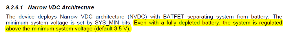
The Sys Output of bq25890 should always above the SYS_MIN (defalult 3.5V).

What's wrong with that?

I have a BUCK DCDC to convert SYS_VCC to 3.3V after bq25890, since the voltage is below 3.3V, the whole system cannot work!

Please help!

Frank

  • Hi Frank,

    The charger can only regulate to SYS_MIN if power is attached to VBUS and HiZ bit =0.  Is power attached to the charger?

  • Hi Jeff,

           Thank you very much for reply.

           I think I misunderstood the SYS_MIN. I thought it can keep VCC_SYS>SYS_MIN even when the system is only powered by the battery.

           I think the datasheet didn't make that clear.

           Does TI have any other charger chip have that function? (keep VCC_SYS>SYS_MIN even when the system is only powered by the battery)

           Thank you.

    Frank

  • Frank,

    I am not aware of a battery charger on the market, from TI or other vendors, that provides SYS_MIN even when no power is applied to the charger.
  • Hello guys!

    I have exact the problem...

    The datasheet is clear!
    "Even with a fully depleted battery, the system is regulated above the minimum system voltage (default 3.5 V)."

    And the graph too!

    If I'm not dumb, this means that if Vbat drops below Vsys_min, the BQ25890 should regulate Vsys above Vsys_min.
    Nowhere in the datasheet is written that there must be any power connected on Vbus... (if it is, on which page?)

    So... Jeff F, it's your turn.

  • Hey Jure,

    Thank you for your suggestion. I do agree the datasheet wording in that section could be improved for our customer's sake, and we will attempt to improve the wording for the next revision.


    I would also like to point out a couple of things:

    1) In our electrical table, the condition to maintain Vsys(min) is the following: V(VBUS_UVLOZ) < V(VBUS) < V(ACOV) and V(VBUS) > V(BAT) > V(SLEEP), TJ = –40°C to +125°C and TJ = 25°C for typical values (unless otherwise noted).

    2) According to our block diagram, our topology is that of a buck converter with an NVDC architecture, meaning a FET (Q4) is placed between SYS and BAT. To be fair, the bq25890 can also operate in boost mode, or what we call "OTG" mode by in effect operating the buck topology in reverse. However, this takes the same two FETS, (Q2 and Q3) to provide the switching action to "boost" the voltage up to at the PMID and VBUS pins. As such, the boost feature which would be required to maintain SYS at a minimum system voltage does not exist between the BAT pin and SYS pin.


    I hope this clears up any confusion!


    Regards,
    Joel H
  • You did :)
    Thank you, Joel!
  • I concur with Joel that this is completely unclear in the data sheet and we design our board with NVDC power path management which doesn't actually exist.
  • Hey Bryan,

    The power path management operation of our chargers which are NVDC refers to two important phenomenon:

    1) Maintaining a system voltage at or above a minimum (typically 3.5V). This voltage moves up with the battery voltage once the battery voltage is above this point. The purpose is to allow the buck converter's regulation point to follow the voltage of a charging battery. The 'NV' in NVDC stands for 'Narrow Voltage', relating to the small potential difference between the battery voltage and the system voltage when above that minimum system voltage. This was designed for applications where a system still needs to operate while also charging the battery (i.e. smart phone, tablet, etc), where most processors have some UVLO below this value.

    2) The ability to re-allocate power away from charging in order to prioritize the regulation of the system, in the event that the input source becomes overloaded. 

    3) In relation to (2), in extreme overloading of the input source, allowing the battery to step in and provide current to the system load. 

    The key here is that there is only a single DC/DC converter with most charger designs, and this single converter can only run in one direction at a time.

    For a good summary of different charger topologies, please refer to this very well written blog: Click Here

    Regards,

    Joel H

  • On page 6 the SYS pin is described as:

    "System connection point.
    The internal BATFET is connected between BAT and SYS. When the battery falls below the minimum system voltage, switch-mode converter keeps SYS above the minimum system voltage. Connect a 20uF closely to the SYS pin."

    This is very misleading, it makes the designer think that SYS will be kept above minimum system voltage as the battery is depleted, which isn't actually true. SYS follows the battery voltage down indefinitely (usually ~3.0V before battery damage). The description does not qualify that SYS will only be kept at minimum system voltage when the charger is plugged in.
  • Bryan,

    Thanks for pointing this out.  I will change to say "When a power source is applied at VBUS and the battery falls below....