This thread has been locked.

If you have a related question, please click the "Ask a related question" button in the top right corner. The newly created question will be automatically linked to this question.

LM27762: Startup issues for invertor, layout question

Part Number: LM27762

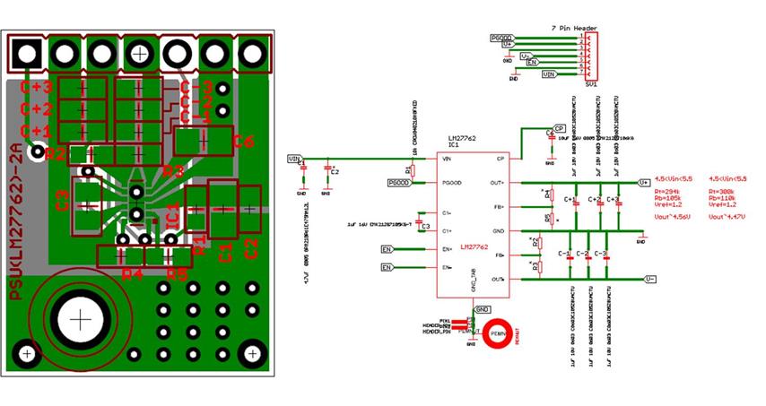
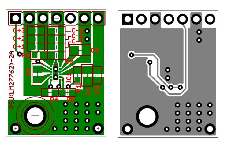
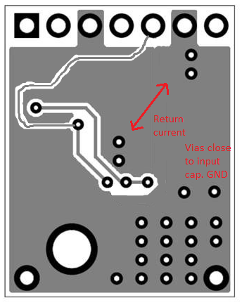
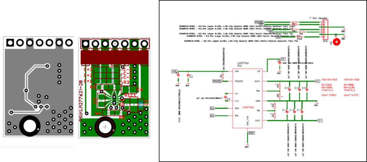
I have been having similar issues to this post (e2e.ti.com/.../582389 ). My question is that I have connected the GND pin to the thermal pad, which is obviously a very close trace. The attached diagram shows that the thermal pad has two vias to the ground plane on the bottom layer. My question is - even though my trace from the ground pin out to the Cout capacitor is long and narrow, shouldn't the thermal pad via's do the trick for avoiding this inductance issue? If so, what else could cause startup issues for this chip?

My design allows either a ~4.8V USB source or a 5VDC source form a voltage regulator. The USB connection starts up without issue, yet the 5V source always starts up in a fault state with the negative output being much too low and the circuit ringing. If I start up with the USB source and then transfer to the 5VDC source without power interruption the circuit runs fine. As well, I can short the negative output momentarily and then the circuit will run fine once I remove the short.

  • Hi Mory,

    The link you are referring to seems to not work anymore, but I assume it was about similar start-up issue you are describing in your post.


    You are correct in that the trace from ground plane is short as you have two vias in thermal pad and GND pin is connected to thermal pad. You have also two vias close to GND pin of output capacitor (C6). Is this 2-layer PCB? I am not sure, but it looks like there is no solid GND plane between those groups of vias. If this is true, then return current from output capacitor has to go long way around PCB.  There is also trace between GND pin and capacitor on the top layer, but that seems to be too long. Can you share the picture of bottom layer?

    The fact that it works with lower Vin makes sense as the rush current at start-up is smaller with low Vin.

    Regards,

    Juha

  • Juha,

    See both layers below. Note that there are two header pins for ground and they are connect on the main board that this test board connects to.

    Looking forward to your suggestions.

    M

  • Thanks for the layout images. See my proposal below:

    - I would re-route one track (enable I guess)

    -I would add vias next to input capacitors to GND plane.

    -I would also move C6 closer to LM27762. You can remove GND trace on top layer between LM27762's GND pin and C6's GND terminal as there is connection to GND plane anyway.

    You can also refer to the layout example in the datasheet.

    Regards,

    Juha

  • Here is version 2 of my PCB layout. Still having startup issue with negative side. Seems to startup ok a bit more often then the first version, but still happening.

    Any ideas?

  • Hi Mory,

    Your layout looks much better now. I can't see capacitor values in schematics - text is so small. Do you have BOM? I am also interested in  exact type of capacitors you have used.

    Regards,

    Juha

  • Part Value Part #
    C+1 1uF 10V 0603  LMK107B7105MA-T
    C+2 1uF 10V 0603  LMK107B7105MA-T
    C+3 1uF 10V 0603  LMK107B7105MA-T
    C-1 1uF 10V 0603  LMK107B7105MA-T
    C-2 1uF 10V 0603  LMK107B7105MA-T
    C-3 1uF 10V 0603  LMK107B7105MA-T
    C1 4.7uF  0805 GRM21BR61E475MA12L
    C2 1uF 10V 0603  LMK107B7105MA-T
    C3 1uF 16V  EMK107B7105KA-T
    C6 10uF 16V 0805  EMK212BJ106KG-T
    IC1 LM27762 LM27762
    R1 10k 0603 CRCW040210K0FKED
    R2 105k 0603 302-105k-RC
    R3 287k 0603 ERJ-3EKF2873V
    R4 287k 0603 ERJ-3EKF2873V
    R5 105k 0603 302-105k-RC
    R6 0 OHM JUMPER 0805 RC0805JR-070RL - 0.0 Ohm Jumper
    R7 0 OHM JUMPER 0805 RC0805JR-070RL - 0.0 Ohm Jumper
    R8 0 OHM JUMPER 0805 RC0805JR-070RL - 0.0 Ohm Jumper
    R9 0 OHM JUMPER 0805 RC0805JR-070RL - 0.0 Ohm Jumper
    R10 0 OHM JUMPER 0805 RC0805JR-070RL - 0.0 Ohm Jumper
  • I have provided the BOM as requested, indicating capacitor part #'s. Can you comment either way if any capacitor selections may be problematic and/or indicative of my IC startup issue?

    Thanks

  • Mory,

    Sorry for late reply. Your components seem to be ok. If you are willing to try yet another layout modification, you can try rotating input caps C1 and C2 and charge pump output capacitor C6 so that their ground pins join already in top layer. then connect that node with several vias to GND plane. That should improve situation further.

    I am not supporting charge pumps anymore, so I will assign this thread to new support person.

    Regards,

    Juha