This thread has been locked.

If you have a related question, please click the "Ask a related question" button in the top right corner. The newly created question will be automatically linked to this question.

TPS65094: system shut down issue

Part Number: TPS65094

Hi Team,


Sorry to bother you. We have a system shut down issue in my customer’s new project, may I have your comment or suggestion?

Customer mention their system would be holed in code-84 when Intel CPU’s temperature higher than 60°C (in system start up process). After we checked it on customer’s board, the output of VCGI power rail would drop to lower voltage level when this issue happened.

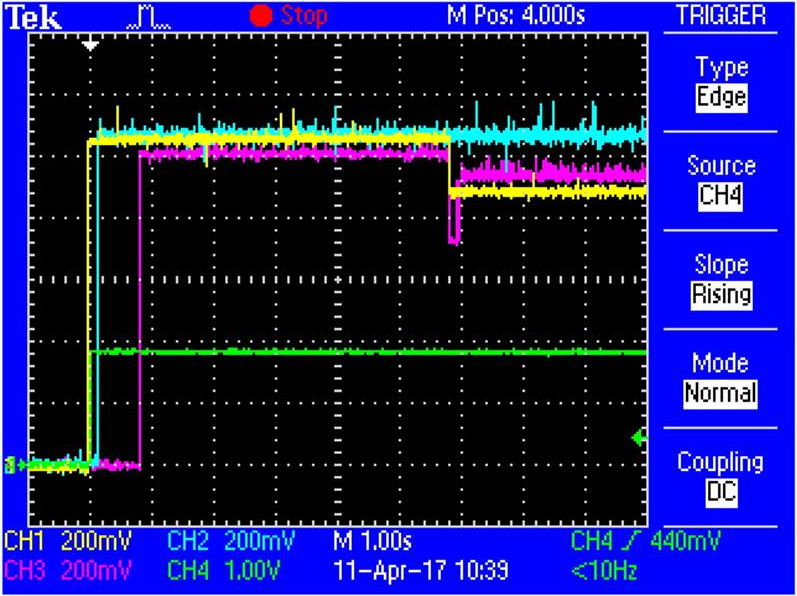
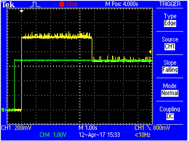
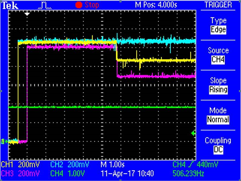
Please refer to below waveform, we could capture the different waveform between good and failed behavior. Do you have any idea or previous debug experience for this kind of issue? Or any condition will pull low +VCGI_Vout by our PMIC?          

CH1= +VNN_Vout

CH2= +V1.05S

CH3= VCGI_Vout

CH4= I2C DATA

waveform 1. Failed waveform => VCGI_Vout would be pull low. 


waveform 2. Good waveform => VCGI_Vout could been pull high after a low pulse signal. 

  • Hi Redick,

    I don't think there is enough resolution with these division size to see the 1 MHz (1 us period) signals on the SDA line. The VCGI rail starts at 0 V and is set to a voltage by I2C, so there must be I2C commands at least during initial power up of VCGI rail. I suspect there are also I2C commands as the VCGI is set low, otherwise the part would power fault and shut down all rails. They will need to identify why the processor is setting our voltage low (if the I2C command is present).

    In the bad case, the SDA line is already high; is the top image coming out of SLP_S3 while the bottom image is cold boot? Is this intended? Does the issue show up in both cases?

  • Hi Kevin,


    Thanks for your reply.

    Both of images are cold boot process, the difference is temperature. Top image is 60°C (CPU) and bottom is normal.


    Yours Faithfully

  • Hi Redick,

    Perhaps that is the problem. The first image does not appear to be cold boot. We can see that the SDA line is already pulled up to 1.8V prior to VNN being enabled, which should not be happening in G3 state when V1P8A is disabled. What is the state of the PMIC_EN pin? Perhaps the embedded controller isn't properly setting the system into G3, but staying in S5 instead?

    The difference between the two is clear in the image. In a cold boot, the VNN is enabled first, while V1P05 (also known as VCCRAM) is enabled much later (see Figure 6-7 in the datasheet). This is visible in the second, correct sequence.

    For a non-cold boot power up (from any SLP_Sx to active), the VNN and VCCRAM (V1P05S) are enabled with only 2 ms delay. Figure 6-9 and all the figures after it show this behavior.

    The difference between cold boot and start from S5 is important because of the VNN rail timing.
  • Hi Kevin,


    I have captured the waveform of PMICEN, SLP_S4B, SLP_S0B and SLP_S3B as below.

    But I didn’t see any abnormal waveform on it, thanks a lot.


    CH1: +VCGI_Vout

    CH4: PM_SLP_a_S3


    CH1: +VCGI_Vout

    CH4: PMICEN


    CH1: +VCGI_Vout

    CH4: PM_SLP_a_S0

    CH1: +VCGI_Vout

    CH4: PM_SLP_a_S4


    Yours Faithfully

  • Hi Redick,

    PMICEN is high in the second image. This is not a cold boot, it is sleep state S5 to S0 transition, shown in Figure 6-11 of the datasheet. If they are expecting cold boot, then the EC is likely having an issue given that it is not setting PMICEN low.