This thread has been locked.

If you have a related question, please click the "Ask a related question" button in the top right corner. The newly created question will be automatically linked to this question.

UCC28251 Vpre-bias and external clock

Other Parts Discussed in Thread: UCC28251

I have questions about UCC28251.

Question 1 : 

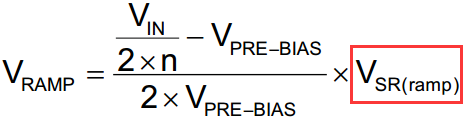
This question is about dataseet p.32  formula(22).

     Vramp={Vin/(2 x n)-Vpre-bias} / (2 x Vpre-bias ) x Vsr(ramp)

Please tell me the optimum voltage of Vpre-bias under the following conditions.

    Vin=180~210

    Vout=125

   Iout=1.6A 

Question 2.

We try to use the external clock.

    - Please tell me the relationship between registor of RT pin and external clock.

    - Please tell me the peripheral circuit that applys to RT pin.

    - Please tell me the timing of applying the external clock.

    - Please tell me the notes when the IC starts to enable.

Best regards,

  • Hi Takahiro-san,

    I have asked one of our application engineers to respond to your question. You should see a response soon.

    Regards

    Peter
  • Hi Peter,

    Could you let us know the current status of this?

    If you need any futher information, please let us know.

    Thanks,

    Regards,

    Kai

  • Hi Kai,

    The the highest pre-bias start-up voltage required by the system, genernally 90% of output voltage but it depends on the customer.

    The UCC28251 can be synchronized to an external clock by applying a narrow pulse to the RT pin. Usnally the external clock must be at least 10% higher than the free-running oscillator frequency set by the RT resistor. if you have too much difference between sync and initial frequencies, then the PSU may damage if the SYNC signal is lost. So the RT resistor is always required, whether the oscillator is free running or externally synchronized

    The synchronization pulse can be coupled into the RT pin directly or through a small capacitor to ensure the pulse width at RT is less than 50% of the clock period under all conditions. When the synchronizing pulse transitions low-to-high (rising edge), the voltage at the RT pin must be driven to exceed 1V. During the clock signal’s low time, the voltage at the RT pin should below 0.2 V. The UCC28251 aligns the turn-on of primary outputs OUTA and OUTB to the falling edge of the synchronizing signal, as shown in Figure 25 in datasheet.

    In addition, when programmed by RT resistor, the minimum switching frequency can be as low a 27 kHz. However, when synchronized to an external frequency, the internal oscillator frequency is clamped to 84kHz during synchronization if the external source frequency drops below 84 kHz, so the minimum switching frequency can is 42 kHz at this time.

    Thanks
    Oliver
  • Dear Mr. Oliver

    Thank you for your answer.

    I have a question about the formula (29).

    You said Vpre-bias is 90% of output voltage.

    Vpre-bias=125(Vout)×90%
    =112.5

      (29) VRAMP= {Vin / (2×n)‐V_PRE-BIAS} / (2×V_PRE-BIAS)×VSR_(ramp)
            = {180 / (2×0.385)‐112.5} / (2×112.5)×3
    =(233.7-112.5) / 675
    =121.2 / 675
    =0.1795

    Is the calculation formula correct?


    Best regards,


    Nishizawa
  • Please notice the VSR(RAMP) is the numerator, the calculated results should be ~1.62V based on your parameters, please double check.

  • Dear Mr. Oliver

    Thank you for your answer.

    I want to ask you questions.


    Question 1.

    About external clock, Does the IC have the limit of duty cycle?

    Question 2.

    About external clock, We try to use silicon oscillator, inputs 3.3V to RT pin.
    Is there a problem with this method?


    Best Regards,


    Nishizawa
  • Dear Mr. Oliver

    Thank you for your support!

    How is the answer of our question going?
    I am glad that you will tell us your answer as soon as possible.


    Best regards,


    Nishizawa
  • Hi Takahiro-san,

    See my response below your questions:

    Question 1. About external clock, Does the IC have the limit of duty cycle?

    The IC does not have limitation on the duty cycle of external sync signal, but the PWM duty cycle can't exceed 50% under all conditions.

    Question 2. About external clock, We try to use silicon oscillator, inputs 3.3V to RT pin. Is there a problem with this method?

    No problem if follow the instructions above: When the synchronizing pulse transitions low-to-high (rising edge), the voltage at the RT pin must be driven to exceed 1V. During the clock signal’s low time, the voltage at the RT pin should below 0.2 V. External frequency source ranging from 84 kHz to 1.89 MHz, which is equivalent to an 42-kHz to 0.945-MHz switching frequency.

    Best Regards
    Oliver