This thread has been locked.

If you have a related question, please click the "Ask a related question" button in the top right corner. The newly created question will be automatically linked to this question.

TLV1117LV: failed devices

Part Number: TLV1117LV

Hello,

We are having some issues with the TLV1117LV33 in one of our products. The LDO has a nominal input of 5V, generated by a buck converter. The output is used to power a PLC chipset (microcontroller + AFE).

A few units have been returned with bad 3.3V rails. The measured rail voltage was only about 1.5V instead of 3.3V. After disconnecting the LDO from the load (there is a 0ohm resistor on board), the LDO output increases to about 4.4V. Replacing the LDO fixed the problem on the devices. We did not find any other failed components on the 3.3V rail or 5V rail. There is no visible sign of damage on any of the parts or the board.

We did several tests to try and determine the cause of the failed LDO's, but have not found the root cause. So far, overvoltage seems to be the only reasonable explanation, although we would expect other components on the 5V rail to fail much sooner than the LDO. We also did some tests with the 5V buck converter and found it very hard to generate any significant overshoot (startup, load transient, input transient, ...). We do have another theory that oscillation may be an issue. The devices have backup power (super caps) which is generated by a boost converter, which in turn powers the 5V buck. A sudden change in load at the end of the 'last gasp' can result in the rail voltage oscillating slightly. Meaning it suddenly jumps back up due to the load dissapearing. Though this also does not cause any significant overshoot.

We also did a controlled overvoltage test on the LDO to see at what point it tends to fail and found that the 6V rating in the datasheet is very conservative, so it seems unlikely that a small amount of overshoot would damage the device permanently.

As for other possible cause, the device has overcurrent and overtemperature protection so those seem unlikely. Furthermore, the 3V3 rail is normally never loaded excessively.

The LDO has a 2.2uF input cap and a 10uF output cap.

Questions:

  1. What would typically cause this type of failure mode (LDO voltage too low under load, too high without load)?
  2. Can 'oscillation' or a varying input voltage cause damage to the device (seems unlikely)?
  3. I've heard it's possible to do failure analysis at TI.
    1. Do you think this would be appropriate in this case?
    2. What would be the approximate cost for us?
    3. How long does failure analysis typically take?

Kind regards,

Sam

  • HI Sam,

    Would you mind sharing a schematic? I am interesting in seeing how the super-cap and buck are used. Is the super-cap on the input or output of the LDO? Any scope plots you can share showing power up, power down along with the transitions to and from back-up power would help us to better understand what may be happening.

    This is the first I have heard of this type of failure mode, so their may be some unforeseen stress on the device in the application.

    Also, I would encourage you to contact your local sales support to submit the devices for failure analysis.

    Regards,

  • Hello John,

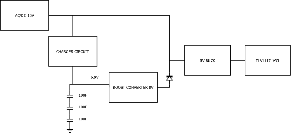
    I can show you a block diagram, but unfortunately I am not allowed to share any detailed schematics publically.

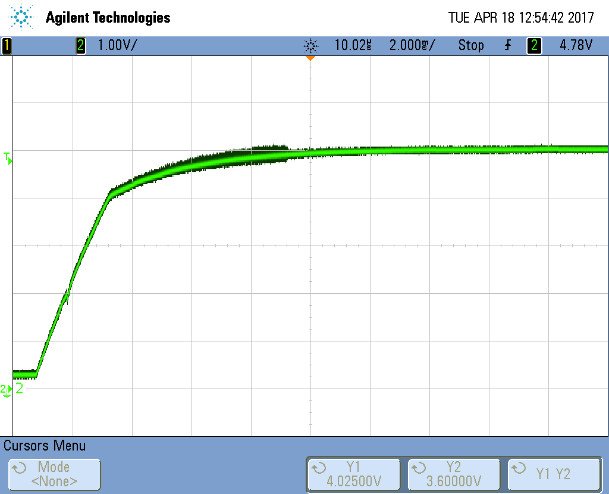
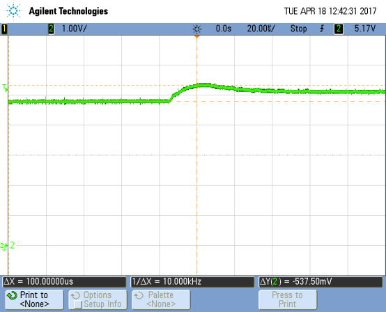
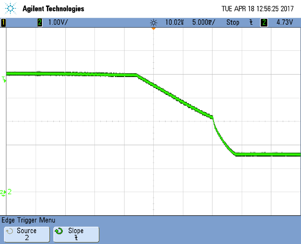
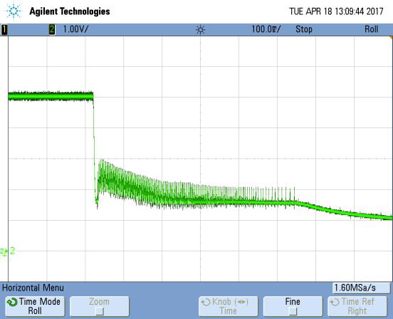
    I have some measurements of the 5V rail:

    Startup behavior:

    2.3A load step:

    normal shutdown:

    last gasp (backup power shutdown):

    Here is another capture of startup (both 5V and 15V rail):

  • HI Sam,

    Thank you.

    I do not see anything to be concerned about here. How about the VIN and VOUT startup/shutdown behavior of the TLV1117LV? Is there any chance either of these voltages are going negative or do you see VOUT being greater than VIN during shutdown? Just wondering if there is a pulse of reverse current going through the parasitic body diode of the LDO FET.

    How much total capacitance do you have at VIN and VOUT of the LDO?

    Regards,
  • Hi John,

    Yes, I forgot to mention that is also one of the things we have considered.

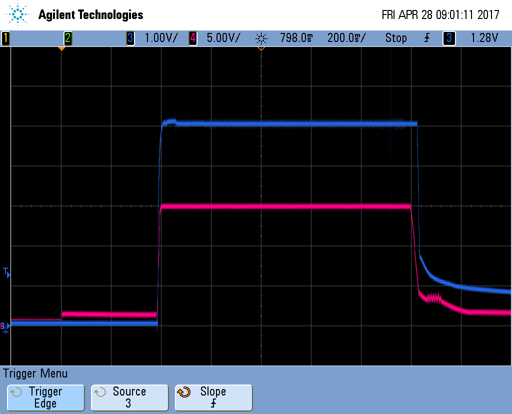
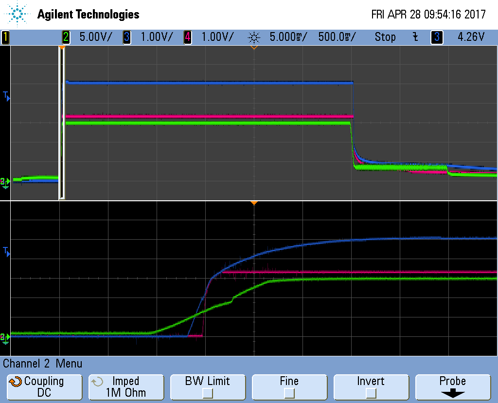
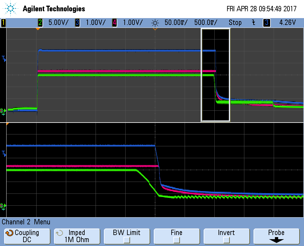
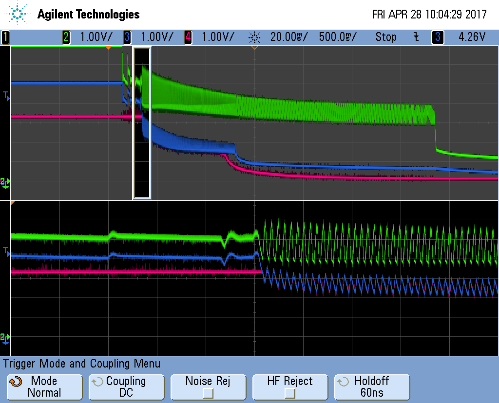
    I have some plots of the 3 voltages (green=15V,blue=5V,pink=3V3).

    Startup:

    Shutdown:

    3V3 seems to follow 5V exactly, which rules out reverse current because otherwise there would be a diode drop difference between the two. Am I right about this?

    Here is the behavior at backup power shutdown:

    Again the 3V3 seems to follow 5V exactly, no diode drop.

    We did some test before with a TLV1117LV without any load and a large output cap. We unplugged the device and expected there would be a reverse current from the cap discharging to the 5V rail, but the device seemed to have no issue with reverse current going to the 5V rail.

  • Hi Sam,

    Thanks for the scope shots, they are very helpful. Looking at the zoomed in portion of the last scope shot it's possible that there is some reverse current events occurring but it's hard to tell. If you look closely you can see places where the pink trace is higher than the blue trace this could simply be due to the limited resolution since we are zooming in on a waveform that was sampled at a lower frequency. If you can it would be great to re-look at this portion of the waveform without using the zoom feature of the scope so that the time per division is much smaller and therefore the sampling frequency is increased for a cleaner image. 

    If you can it would be great to re-look at this portion of the waveform without using the zoom feature of the scope so that the time per division is much smaller and therefore the sampling frequency is increased for a cleaner image. 

    -Kyle

  • Hello Kyle,

    Thanks for the tips.

    I have some more scope plots that show the waveforms in greater detail.

    Meanwhile I have also connected a short loop of wire at the input pin of the LDO to measure the current with a current probe.

    I think we indeed have some reverse current spikes at shutdown.

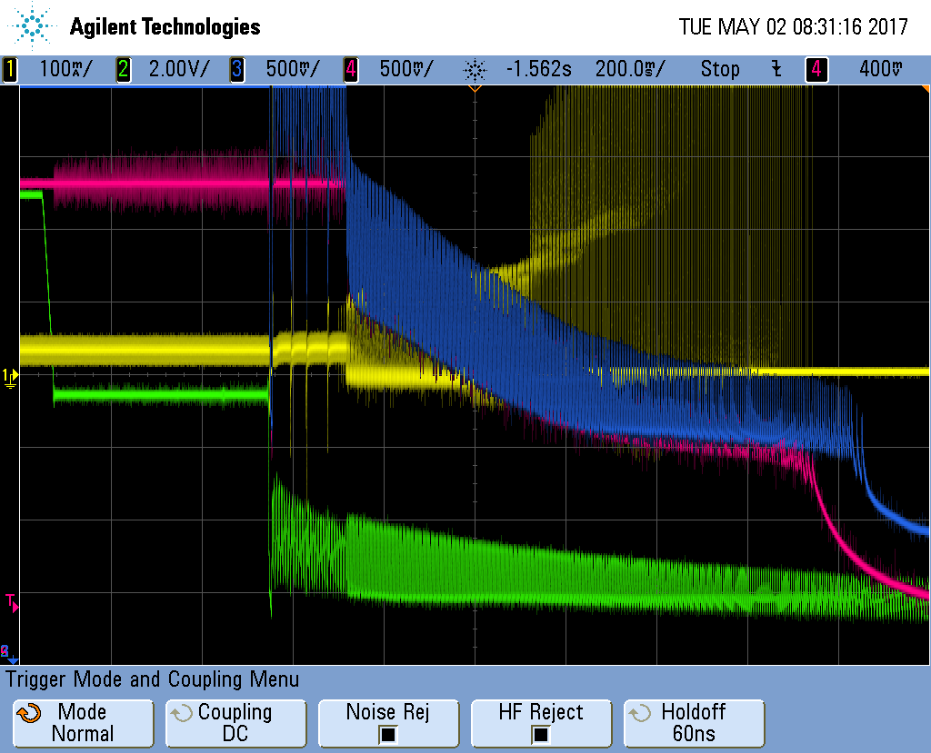
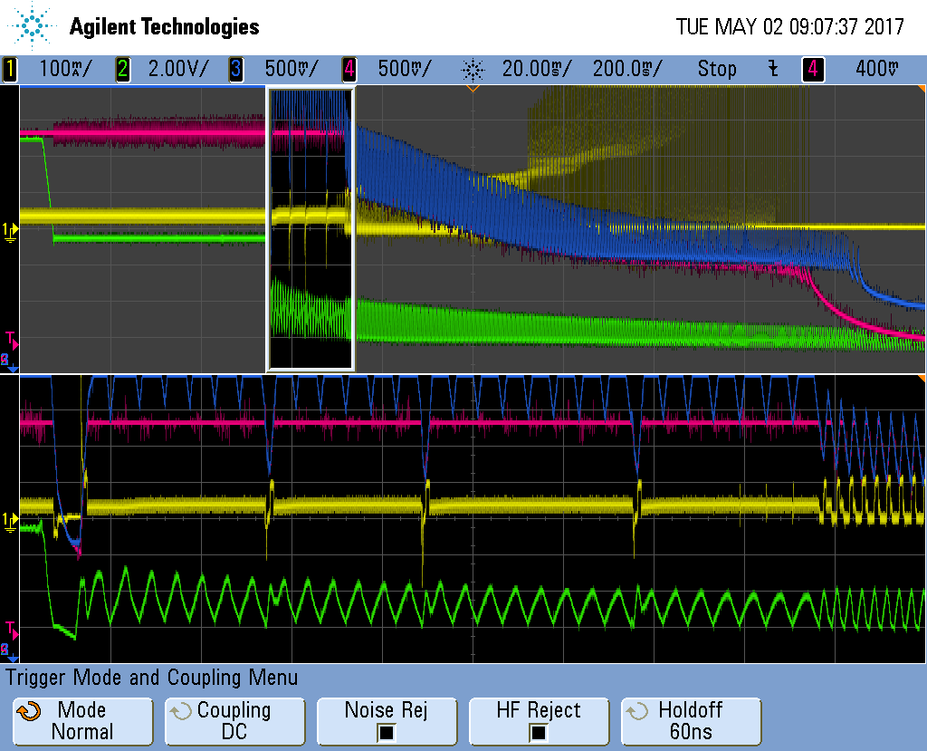
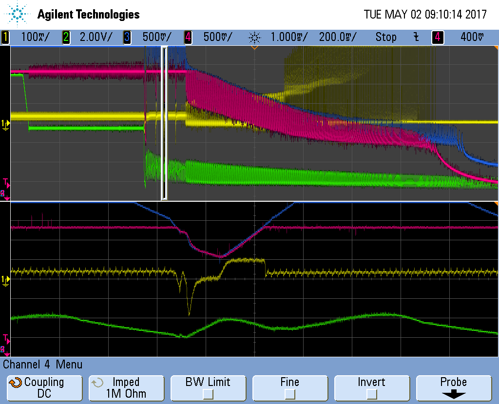
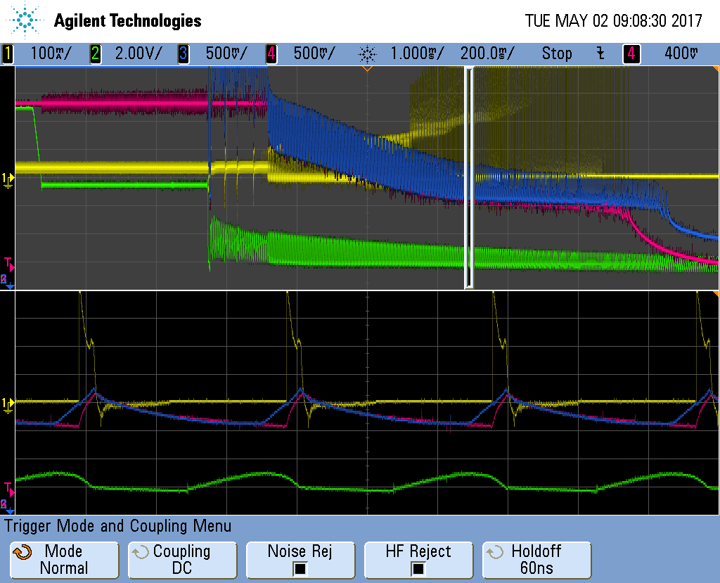
    Colors are: Yellow=current at input pin of the LDO,green=15V,blue=5V,pink=3V3

    Following shot gives an overview of the shutdown.

    Next shots show the highest spikes (about -200mA)

    There's also some reverse current later in shutdown (about 100mA):

    The datasheet mentions the following regarding reverse current:

    The PMOS pass element in the TLV1117LV device has a built-in body diode that conducts current when the voltage at OUT exceeds the voltage at IN. This current is not limited; if extended reverse voltage operation is anticipated, external limiting to 5% of the rated output current is recommended.


    What does "extended reverse voltage operation" mean in this context? The reverse current peaks last for only a few 100µs.

    Would you expect damage to the device at these kinds of currents? We have only had a few failures so far. Any idea what the failure mechanism is like? Does the LDO fail immediately if the reverse current is too high, or does it degrade and then fail? If the PMOS fails, we would expect the output to be basically 0V. In our case the voltage is about 1.5V under load which seems to indicate the PMOS is still able to conduct some current.

  • I just tried breadboarding a circuit in which I forcefully generate a reverse current through the LDO. Something like this:

    I now measure reverse currents of over 1A for roughly 200µs, yet the device seems unaffected.

    It seems very unlikely that such a large reverse current would ever occur in our product. 

    Of course I only tested this on a single device and only a few times, but I'm a bit baffled that the device is not damaged by such a large current considering the 5% reverse current rule of thumb.

    EDIT:

    I did another test using a constant load of 1.5A at the input. No input voltage, 3V3 applied to the output. The device gets very hot, but continues operating fine once I reapply 5V at the input.

  • Hi Sam,

    Some of our devices are capable of handling reverse current for short periods of time that is more than the 5% of the rated current. However, if this is consistently done there is the possibility of degrading the device from a long term reliability stand point. Not all reverse current failure modes occur in such short periods of time, one example of a failure that could occur as time increases is de-metalization due to electromigration. The parasitic paths which the reverse current takes are not sized to handle such large amounts of current and over time the current crowding in these smaller traces can cause voids to form in the metal lines eventually leading to an open circuit. 

    -Kyle

  • Hello Kyle,

    Thanks for your reply.

    I agree that we should avoid this situation in our circuit, possibly by placing an additional reverse diode across the input and output terminals.

    However, the failure mode you are describing does not seem to match what we are seeing in our failed components. So even though it should be fixed, I am not sure it is the cause of the failures we've seen.

    If I'm interpreting this correctly, reverse current would likely cause an open circuit in the main path. So essentially, no current would be able to flow from input to output (aside from any bias or leakage currents).

    What we are seeing, are components where the LDO voltage drops to 1.5V (instead of 3.3V) under load and increases to about 4.4V with no load. Furthermore the diode seems to be intact (I measure 0.7V from output to input using diode tester). And this is pretty consistent across the failed components. So I don't see how an open circuit could cause this kind of behaviour. Or could this be part of the "degrading" you are describing?

    I'm having a hard time trying to estimate how the circuit might behave under these conditions. If it just increases the drain-source resistance, I would not expect the voltage to increase to 4.4V without load. Or is the degrading more like a fundamental change in the I-V characteristic of the PMOS?

    I've tried to reproduce the behaviour we are seeing through simulation, but have had no luck so far...

    EDIT:

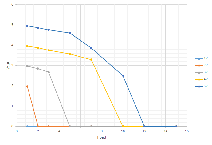
    I did some measurements on a failed LDO. This graph shows the output voltage of the LDO versus the load current at various input voltages. 

    There is no voltage regulation anymore and the LDO isn't able to handle any substantial current at all. Would it be possible to figure out what part of the LDO has broken based on this behaviour?

    I don't know if the internal circuitry is at all similar to the conceptual diagram shown in the datasheet?

  • Sam, 

    Reverse current can cause several different failure modes depending on the magnitude of the reverse current, my previous pos was simply trying to provide one example of a failure mode which could occur due to long term exposure to reverse current situations but doesn't immediately cause the device to stop operating as expected. Your graph indicates that the pass device has much more resistance than when undamaged. This is a common occurrence with EOS damage to the pass device.  

    -Kyle

  • Hello Kyle,

    OK thanks for clearing that up.

    We are going to do some stress tests on 20 of those parts to see if we can reproduce the failures.

    Kind regards,

    Sammy