This thread has been locked.

If you have a related question, please click the "Ask a related question" button in the top right corner. The newly created question will be automatically linked to this question.

TPS62750: instability problems

Part Number: TPS62750
Other Parts Discussed in Thread: TPS61252

Dear,

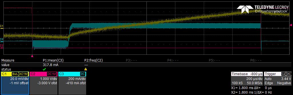
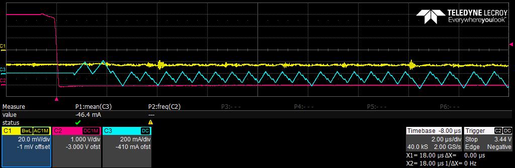
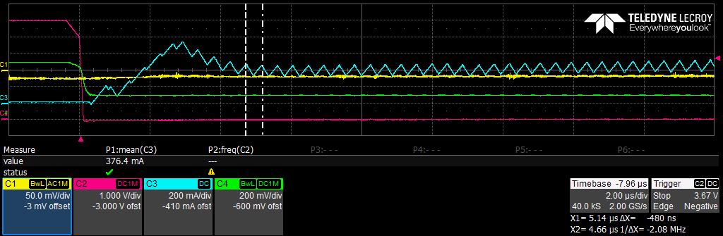
I was wondering if someone with more experience with the TPS62750 could help me with some instability problems that I have.

The DC/DC converter works fine when the H/L pin is in high level, but it does not when this pin is in low level. The resulting waveforms are not those expected and moreover the circuit consumes around 10-15 mA when no load is connected to the output. I suppose that the circuit becomes unstable, but I do not know why. And this is just when H/L pin =0!!

Any advice to solve this problem?

With regard to the PCB layout, I followed the advices indicated in its datasheet.

Best!

Ferran

  • You can always order the EVM to obtain a known good working circuit.

    This app note explains a good test setup for measuring PFM mode efficiency: www.ti.com/.../slva236.pdf

    Instability is easily confirmed by looking at the key operating nodes with a scope.
  • Dear Chris,

    I’ve been trying to solve the problems that I had with the TPS62750 using a new PCB and following all the guidelines provided in the datasheet (I cannot use the EVM from TI since the DC/DC converter has to be in the same board as the sensor to be supplied), but I still have problems that I am not able to solve:

    -The monitoring of the inductor current shows that there is a negative current (of about 100 mA during 200 us) right after the DC/DC is enabled. After that, the inductor current is well regulated around the desired value.

    -The DC/DC converter does not operate correctly when the H/L pin is in low state, but it does when H/L is in high state, taking into account the previous limitation.

    Do you have any clue of which can be the cause of these problems?

    Thanks for your time,

    Ferran

  • You could use the EVM to compare its behavior and waveforms to those on your board.

    You are able to post waveforms in these threads. It is usually required to examine waveforms in order to debug a circuit.
  • Dear Chris,

    Attached you can see the waveforms (the latter is a zoom of the former) for Vin=6V, Vout=3.3V and Iout=10mA, where:

    Channel 1: output voltage in ac coupling

    Channel 2: FB signal. In my circuit the output voltage is on purpose monitored by a comparator (with hysteresis) that activates the DC/DC converter through the FB input.

    Channel 3: Inductor current measured by a current probe.

    Note that at the beginning the inductor current is negative, i.e. the current goes from the output to the input. I’ve found your article “testing tips for applying external power to…” which says that in the TPS62750 this current path should not be possible.

    Do you have any idea of why the current evolves in such a way?

    Best regards,

    Ferran

  • Can you show how you are driving the FB pin? If this is the red trace, it seems to go from several Volts to 0V. It should be at 600 mV for the IC to be regulating.

    When FB first goes low, the IC is sinking current for a brief time to reach the new Vout setpoint. This is why the inductor current is negative.

    The app note refers to the 'reverse current protection' section of the D/S, which applies when the device is disabled.
  • Yes, the FB pin is driven by the red signal.

    We are trying to do something similar to what was done in:

    Here, we did it with a boost dc/dc (TPS61252) and the circuit (please, see fig. 5 of that paper) work as expected. In other words: when the FB pin had a low signal (around 0 V), the converter transfered energy from the input to the output at the maximum inductor current determined by a resistance.

    However, it does not work with the TPS62750, and I do not understand why.

    Anyway, thanks again for your feedback!

  • Thanks for explaining.

    Is it possible to modify your test setup so that the FB pin is not driven so far away from its typical operating point? Driving it just ~10mV from 0.6V should be all that is needed to start or stop switching.

    For example, keeping your circuit as it is now, you can add a voltage divider from Vout to FB to GND. Then, add a 3rd resistor from FB to the output of the comparator. The comparator can still go fully high/low but this does not equate to a full signal on FB.

    Finally, while this is a different topic than what you are studying, this reference design shows an efficient way to get power out of a very small source, through a neat current limit technique, while still driving a super cap. http://www.ti.com/tool/PMP9753
  • Hi Chris,

    Many thanks for your advice! Today, I’ve proved it and it works properly without the negative current at the beginning!! Look the new response (channel 4 in green line is the actual voltage applied to the FB input, with a high level of around 650 mV and a low level of 300 mV):

    However, the DC/DC converter works correctly only when the H/L pin is in high level.

    When the H/L pin is in low level, again we have a negative current. To be precise:

    When FB is low (i.e. around 300 mV): the inductor current is positive, and there is a charge transfer from the input to the output, as expected.

    But when FB is high (i.e. around 650 mV): the inductor current is negative, and there is a charge transfer from the output to the input. Theoretically, no switching was expected in those conditions. Do you have any smart advice to solve this problem?

    By the way, if finally we get good results from our experiments and taking into account your help for the development of our setup, maybe you would like to be one of the authors of any potential journal/conference publication. Please, let me know.

    Best regards,

    Ferran

  • Glad that is working, with H/L = high!

    With H/L = low, can you post that waveform? The device sounds like it is operating in forced PWM mode, with H/L = low. This will not work for your use case.

    Sure, it's possible to work on the paper together. Thanks for the invitation. Let's discuss this via email or a 'conversation' here in E2E.
  • Hi Chris,

    Last week I sent you an e-mail at: ti_cglaser@list.ti.com

    I do not know if this is an  e-mail that you check regularly, or you use/prefer another one.

    Best!

    Ferran

  • Sure, let me send you a message.