This thread has been locked.

If you have a related question, please click the "Ask a related question" button in the top right corner. The newly created question will be automatically linked to this question.

TPS54020: question about layout guidelines

Part Number: TPS54020

Hi team,

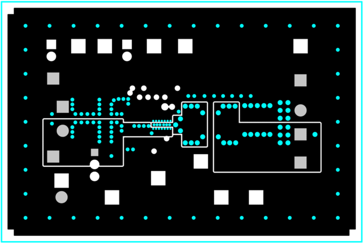
My customer is using the TPS54020 in their latest design. They are not running things very hot, and their max Iout will not get close to 10A. Their board manufacturer is worried about how many vias are all crammed next to each other under the bottom pads of the part. I have two questions:

  • So many vias next to each other will make soldering this part difficult, at least without having solder wick down into the vias. If that happens, is that ok?
  • Since they are not running this part very close to it's max rated Iout or junction temp, can they eliminate a few of these vias?

Thanks,

Brian

  • As you most likely know, the heat is transferred away from the die by the large pads on the IC, the solder connecting them to the land pattern on the PCB ad by the vias from the pads to internal, top and bottom side copper ground, VIN and SW node.  Proper solder coverage is a must.  You can use small diameter vias to minimize wicking.  You can possibly get by with fewer vias.  You would need to perform a detailed thermal analysis to be sure.