This thread has been locked.

If you have a related question, please click the "Ask a related question" button in the top right corner. The newly created question will be automatically linked to this question.

BQ77PL900: Overcurrent breaking BAT and PACK pin

Part Number: BQ77PL900

Hey,

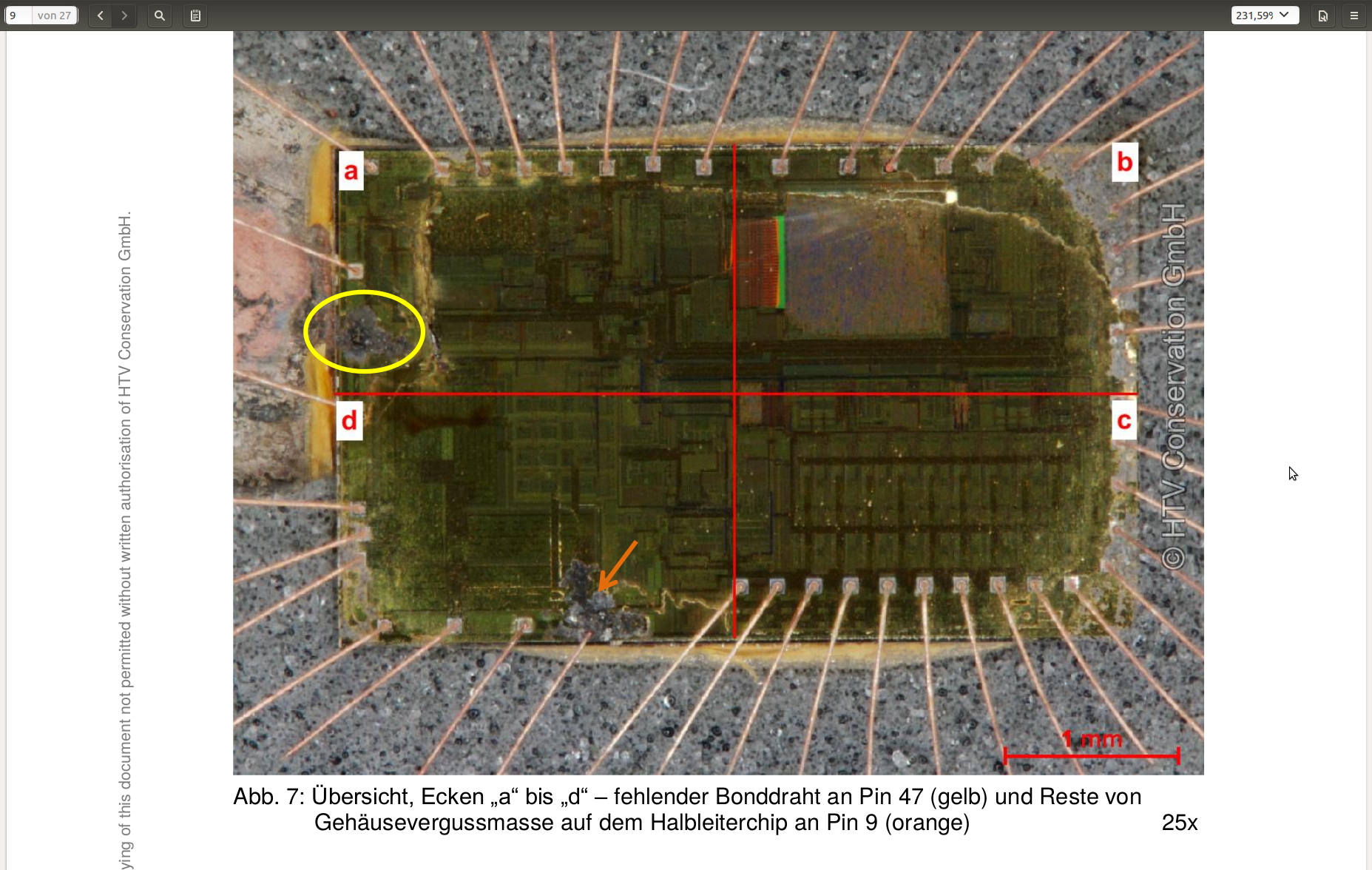
we are using the bq77pl900 with 10 series cells and are experiencing some defects of this chip. The PACK and BAT pin of the chip breaks. There must be some overcurrent flowing into these pins. We chemically opended one broken chip and you can see that defect there. See below.

Right now it's unclear why that overcurrent flows into the chip. I suspect that the "step down charge pump" could have some defect and draws too much current. I did the following tests and checks:

- The three capacitors for the charge pump are ok
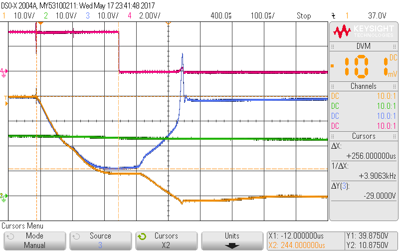
- Tested max load for 5V power supply with constant current of 50mA and ambient temperature of 100°C for several hours.
- Tested max load for 5V power supply with constant current of 50mA and additionally over currents of 100mA for 7,5us with 20kHz. -> Chip temperature rose to 90°C@25°C ambient but chip did not break.

What else could be the cause for the BAT and PACK pin to break?

Ich can give more information if you need.

Thanks very much,

Anton

  • Hi Anton,
    When the battery protects from an overcurrent event the cells and battery interconnect will have an inductive response V = Ldi/dt. Since the filter on the part is small and the hold up circuit (diode) may push current directly into the pins, the PACK and BAT pins may be subject to high voltages and draw high current during the transient. You might inspect the pin voltages during a test sequence with increasing current switching events to see if ratings are exceeded.
    The cell inductance is likely fixed and the interconnect is likely to have a physical size, so may be difficult to reduce inductance. The current is likely also large, short circuit is typically the largest. The switching time may be the easiest to control, the largest time suitable for the safe operating area of the FET is preferred to reduce transients.
    Clamping the pins or increasing the filtering may also be helpful. The difference between the normal operating voltage and the abs max is small but may allow placing a zener or TVS. A series resistance helps limit current into the TVS or filter the transient, but provides a drop with regulator load current which can be undesired since the BAT and PACK pins are also the reference voltages for the FET drive and regulator load current can modulate the gate voltages.
    In some cases it may be desirable to provide transient protection on the battery bus. The EVM used a capacitance on the PACK+ net which would apply to current transients from load switching with less effect on the actual cell transient. Use a transient suppression method suitable for the specific design.
  • Hey,

    thanks very much for you detailed reply.

    Why would there be a higher current flowing into the chip if the voltage at BAT or PACK is higher, but below absolute maximum ratings?

    A possible order of causes I can think of is, that the chip gets an overvoltage, something breaks inside and then the current into the chip rises because of this defect. Is that right? Or is there any other possible cause of a high current into the chip?

    I did some measurements during short circuit protection when the bq77pl900 turns off the DSG-Fet.

    First I measured the voltage at the BAT pin. There is a 4,7uF capacitor close to the chips and I did the measurement at this capacitor. The voltage rises just up to 55V (GREEN) and that is with a current of about 100A. That's close to the maximal possible current. I used a 30mOhm resistor and the battery itself has about 280mOhm internal resistance. The rest of the voltage drops at the PCB. Minimal short circuit resistance in the application is 120mOhm. See scope0.

    Then I did the same measurement for the PACK in over the 1uF capacitor that it close to that pin and there is also no rise in the voltage (GREEN). See scope1. In scope1 the PACK voltage is lower than the battery votlage, because we have a 16V zener diode in from. That is neccessary that we can have a voltage of 12V at the input pin for the charger for compatibility reasons. Otherwise the bq77 would always wake up (voltage at PACK must just be greater that 7V)

    Thanks in advance,

    Anton

    --

    Scope0:

    YELLOW: Voltage at intermediate circuit
    GREEN: Voltage over C64, capacitor at filter of bq77 BAT pin
    BLUE: Battery voltage at input terminal on the pcb
    RED: XALERT of bq77

    Scope1

    YELLOW: Voltage at intermediate circuit
    GREEN: Voltage over C58, capacitor at filter of bq77 PACK pin
    BLUE: Battery voltage at input terminal on the pcb
    RED: XALERT of bq77

  • Hi Anton,
    It is possible that the current to an input pin increases as you approach abs max as long as that current is not severe, but it is unlikely that this current increase is significant. The abs max is generally at a level before where significant current and any risk of damage occurs. As you indicate it would be more likely to have some prior damage to the pin which results in high current approaching abs max. Semiconductors do have other possibilities such as latch-up or triggering a pin ESD protector, but that is not expected on this device within the abs max limits.

    The voltage measured at the BAT pin in the first capture shows the inductive spike described, but only to 55V which is below the pin abs max. Was the part damaged during this capture? It would be good to inspect the routing to be sure the cap is experiencing the maximum voltage on the net. If the route is to the IC pin first before reaching the cap, the IC pin may be experiencing a higher voltage.

    The PACK pin of course does not show a high voltage and should not be at risk from this event. However the description is somewhat concerning if the CHG output is used to control a traditional power FET as shown in the datasheet. Since CHG swings between the PACK pin level and ~ 12V below, if the PACK pin is 16V below the FET source, the gate might be commanded 16V below the source when off and 28V below when on, effectively the FET gate could be overstressed and the FET might be always on. If there is a limiting circuit in place for the gate, be sure it does not feed into the CHG pin and internally to PACK pin. If this happened though I think you would see something on the PACK net at the capacitor.