This thread has been locked.

If you have a related question, please click the "Ask a related question" button in the top right corner. The newly created question will be automatically linked to this question.

BQ25890: EMI mitigation

Part Number: BQ25890

HI, 

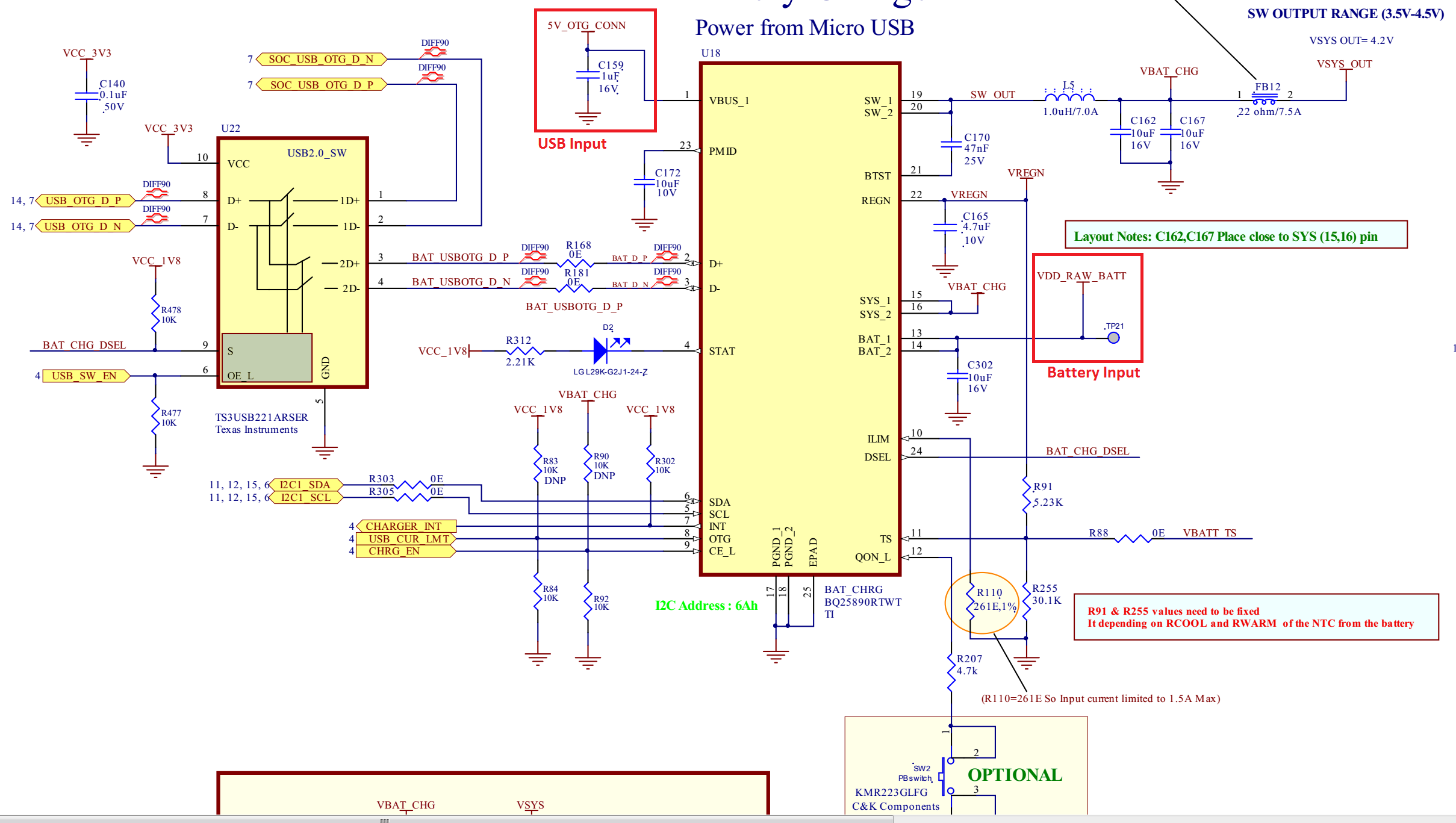
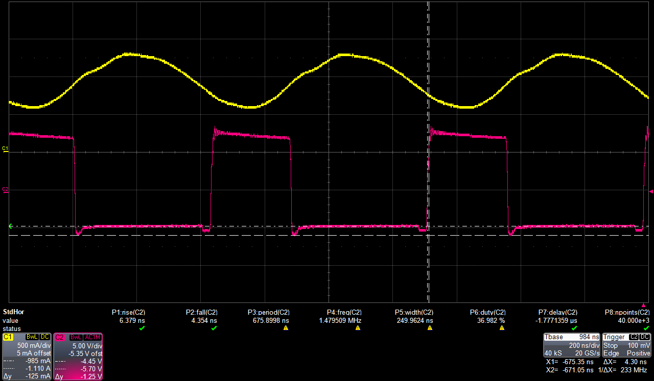
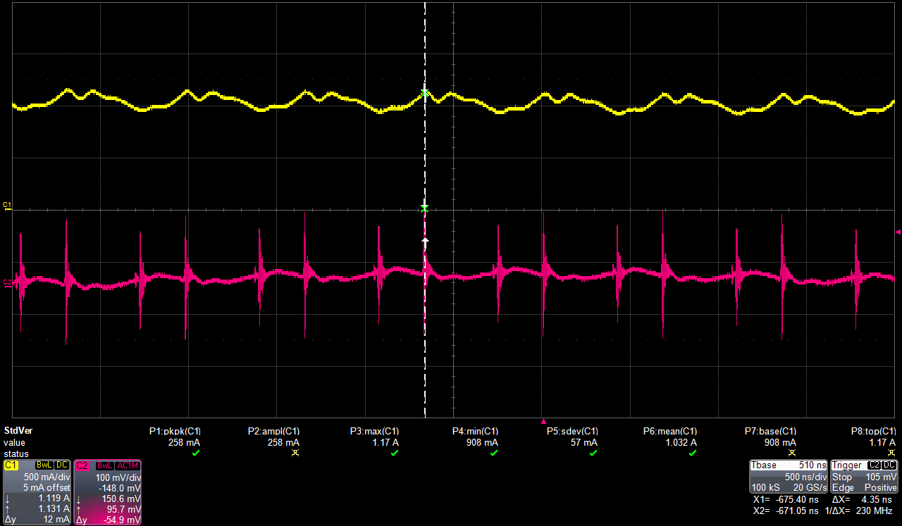
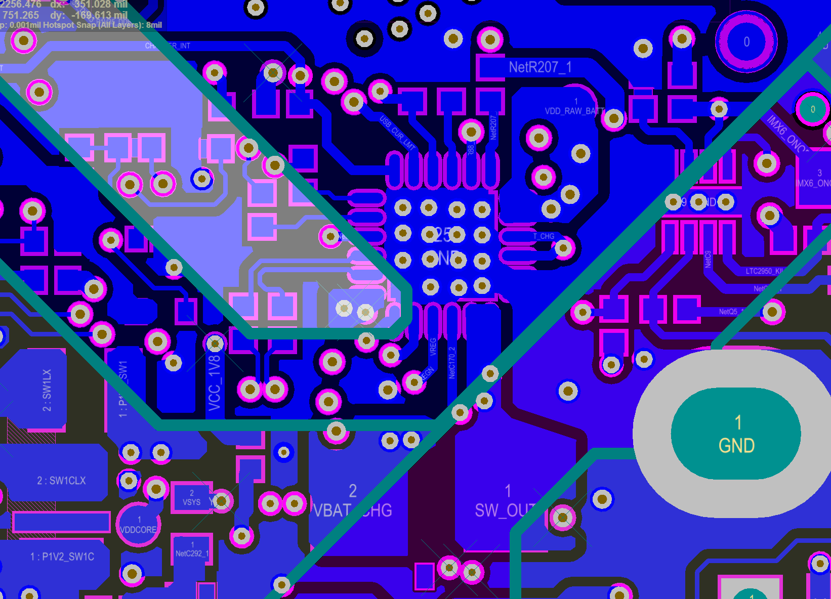
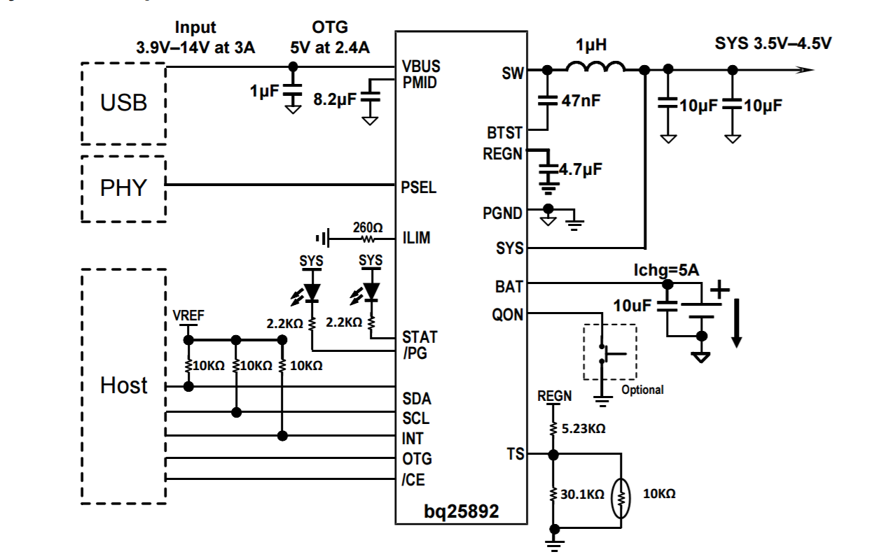
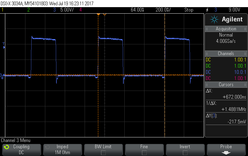
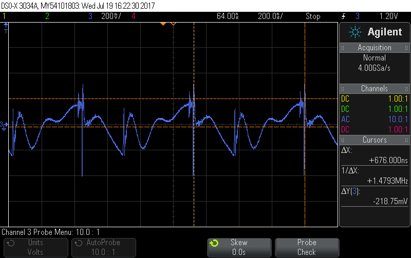
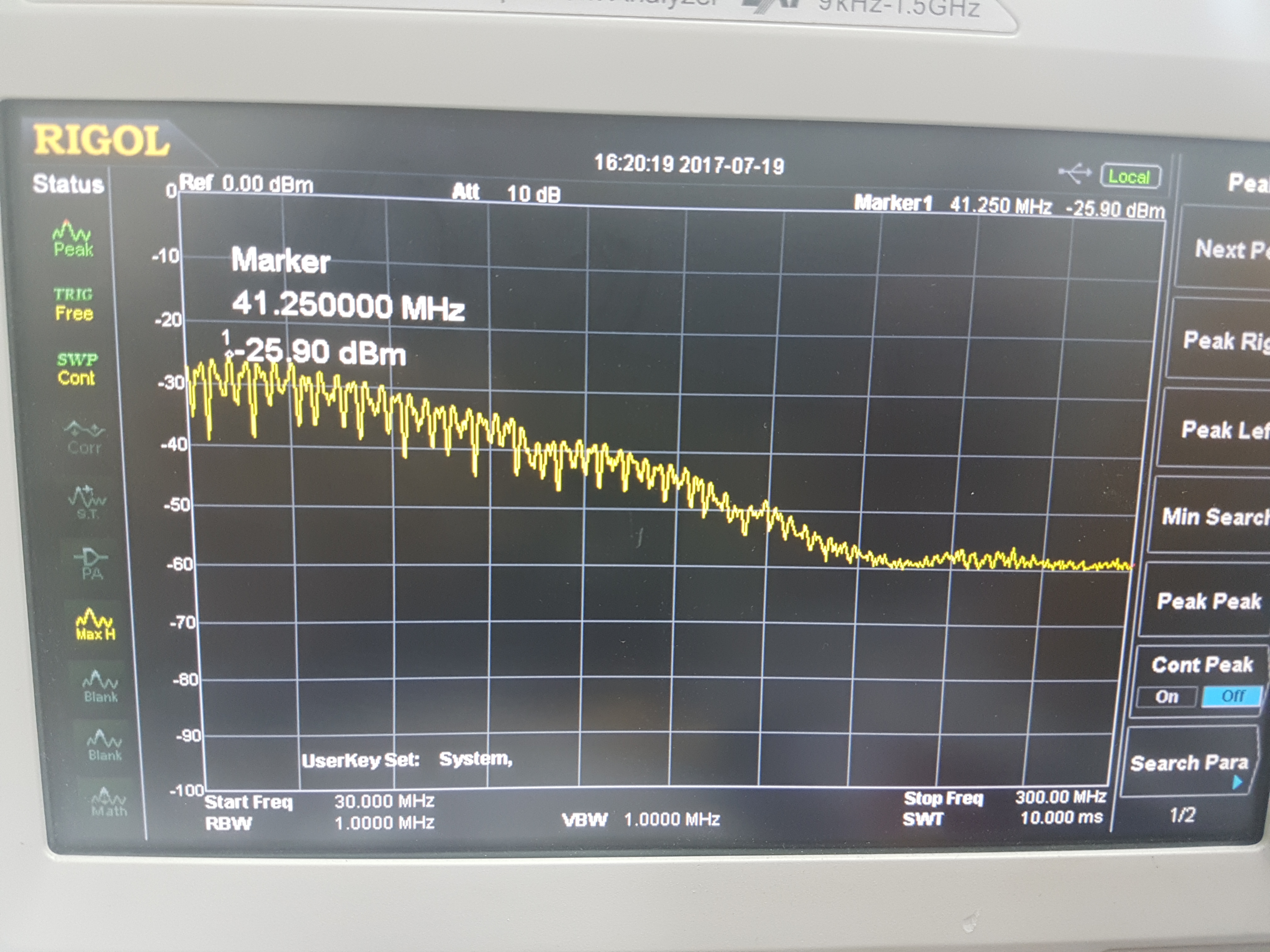
I'm using the bq25890 in my design to charger a 7200mAh battery. In charge mode, my device is failing radiated emission test, and the source of the emission ihas been narrowedd down to the charger IC. Unfortunately this IC does not give enough flexibility to play with the settings (like gate driver slew rate control, etc) 

  • Are there equivalent IC's that have better EMI response that TI carries
  • Are there any suggestions to help reduce the noise level

I'm charging at a rate of 3.5A using a quick charger IC that provides a 11.5V @ 1.5A.  

The device is charging through USB via a wall wart charger (quick charge)

Thanks

  • As with all buck converters, input capacitor placement is critical to lower EMI.  Placing C172 as close as possible between PMID and GND and/or adding a small decoupling capacitor (0.01uF to 0.1uF) usually mitigates EMI.  If not, then adding a properly sized RC snubber from SW to GND will mitigate EMI at the expense of efficiency.  Attached is a document the further explains these recommendations.bq2589xbq2419x_29xlayoutandEMIrecommendation.pdf

  • Jeff,
    Thank you for your reply. I'll give some of these a try and i'll let you know if i have further questions.
  • Hi Jeff

    I have some questions about some the app note as well as my system response. I notice something strange happenning on the switch node. SW_OUT (on my schematic). There is no visible ringing (no overshoot on the rising edge) but there is ~1V undershoot on the falling edge. The strange thing is that the undershoot is held low for some time before recovering, but then right before the start of the rising edge it drops again by approximately the same voltage. The question is why is it behaving like that. I have never seen this. Could this have anything to do with Low side power FET parasitic capacitance ? 

    YEL: input current

    RED: SW_OUT

    I also see some high frequency switching on my input voltage that decoupling capacitors do not seem to remove. I placed a 1nF cap across the 1uF cap on VBUS. The oscillation frequency of that high switching noise is ~230MHz. Do you normally recommend using an LC filter to keep that noise from migrating to the USB charging cable and radiate or you have a different take on it. 

    YEL: input current

    RED: VBUS voltage


    My last question is out of curiosity: 

    How is the switcher being regulated? I don't see on the block diagram on page19 of the datasheet where the error signal is being sensed and how the control loop operates.

    Thanks again for you help. 

  • Your charger is oscillating. I have reviewed the schematic again and don't see any obvious issues. If you remove or short FB12, does the oscillation go away? If you add additional capacitance at SYS or at PMID, does the oscillation go away? If not, can you send your layout and I will review.

    Regarding the feedback error signal, the SYS and BAT pins are the feedback points. There are error amps in the middle left with SYS and BAT points. The control method is a combination of voltage mode and current mode control.
  • Yes, i forgot to mention the oscillation in my previous poIt because i was able to mitigate that with a 10uF on PMID (see screenshot below) I also got similar results adding the same capacitance to VBUS. That being said, from a USB compliance prospective the added capacitance can be an issue (higher inrush current upon insertion of USB, etc) but between VBUS and PMID where do you recommend placing this additional capacitance to lower this oscillation.

    How to do prefer i send you the layout. A 2D screenshot may not give you a good idea of placement. 

    BOTTOM and power plane with copper pour for VBUS 

    TOP


  • Jeff,
    I still haven't gotten an answer about the behavior my switching node is seeing (described in May 19 post), Any thoughts on what's going on there ?or the idea about the LC filter on the input as a way to reduce our switching noise. 

    Also what about the idea of adding an LC filter on the input as a way to reduce our switching noise. What type of care should I take to ensure my LC filter doesn't affect the switcher stability. What's the input impedance at VBUS ?

    Thanks

  • I have never seen this charger oscillate in my 3 years of supporting of it.  Can you send the register settings when you see this oscillation?    In the past with other chargers, adding an LC on the front end usually caused oscillations.  Like any buck converter, the input impedance at VBUS is negative resistance.  I will ask if design has characterized it.

  • Is register 13 bit 7 reporting that you are in VINDPM? If so, if you change your input voltage or change the VINDPM using the Force VINDPM bit (register 0D bit 7) and then changing the value (register 0D bits 0:6), does the oscillation go away?

    Regarding your layout, the single via for PMID from top to bottom is adding a lot of resistance and inductance. That capacitor is the input to the buck converter and so sees large current spikes.

  • Hi Jeff,

    I gave some thoughts to the scope shots I shared with you that showed an apparent "oscillation" of the VBUS line, and input current. Something I forgot to mention in case you have not noticed is the fact that the voltage waveform is AC coupled. The current waveform looks more as if the switcher is in continuous conduction mode and the voltage waveform is more of the

    The current waveform (YEL) looks more as if the switcher is in CCM with quite some capacit

    The voltage waveform (RED) looks more as if it's more of a ripple due to the amount of impedance (charger output impedance) on that path.

    Any additional feedback on the layout woujld be really appreciated.

    Thanks
  • In our current layout, the analog and digital ground are not separated. We are connecting all pins to our system ground. I know the datasheet example block diagram show separate grounds. I'd like to know whether that's necessary?

    Thanks

  • It is not required to separate the grounds.  Many customers do not.  I would not expect combined grounds to cause oscillations or cause significantly worse EMI.

  • Hi Jeff,

    I am about to send my product for certification (FCC) and I have test my product using our spectrum in our lab, I noticed there is  big mountain of frequency from 30Mhz-100Mhz, this only comes out when I am charging BQ25890 12V 1.5A and the host is turn OFF.

    I checked the SW switching and I dont see anything strange please see image SW.bmp. Also I checked the VBUS and a bit noisy( I think its normal). Also, the layout for the PGND are connected in common with other ground, meaning I didnt seperate the PGND.

    I attached the spectrum data for your reference as well the layout for TOP layer second layer I used as power layer for VBUS. There is one ground layer plane on Layer 5.

    SW Output

    Vbus

    Spectrum Data- its around 30dB higher from the noise floor

    Top Layer Layout- Common Ground

    Hi ,

    How did you managed to fix your problem?

    Thanks,

    Jay

  • Jay,

    The attached document summarizes the layout recommendations and additional steps that may be needed to minimize EMI.8475.bq2589xbq2419x_29xlayoutandEMIrecommendation.pdf

    In summary, PMID capacitor placement is the most critical.  Adding a small 0.01-0.1uF PMID capacitor close to IC PMID pin and GND is the simplest potential fix.  Adding a properly sized RC snubber from SW to GND is the guaranteed fix but at the cost of efficiency.

  • Hi jeff,

    Thanks for your reply.

    I think the PMID capacitor is a bit far from the IC and the trace width (layout mistake)is very small do you think this is the root cause?

    I add RC snubber there but seems like 140Mhz area was reduced. The waveform iattached previously is with snubber and 1nF on the PMID but 30Mhz frequency doesnt go down atleast on my spectrum analyzer data which makes me worried that the solution adding RC snubber will not fix in my case.

    Please advise.

    Thanks,

    Jay

  • PMID needs to be close. The snubber has to be specifically sized for your board using the empirical method per appnote mentioned in the presentation. A large enough, even improperly sized, RC snubber will work but it will reduce efficiency.
  • Hi Jeff,

    Thanks for your reply.

    The PMID Capacitor is encircle in yellow on the image below.

    I add different value of RC snubber but the results of the 30Mhz is not improving at all, I see an improvement at 138Mhz which is same as the appnote Page14 Before and After adding RC snubber.

    I am wondering why I don't see improvement on the 30-35Mhz band. I am using a beehive 100C EMC probes I dont have reference if my measurement will exceed the FCC limit. But adding RC snubber as per your suggestion should improve but I don't see improvement on the 35Mhz band.

    Any insight how to further improve? I am seing the PMID capacitor as the major mistake on the component layout.

    Appreciate your help.

    Thanks,

    Jay

  • Hi user4300350,

    May I know what frequency you fail on EMI? and what is the EMC mitigation you have done to fix it?

    I am attaching my spectrum band I am seeing 30Mhz-40Mhz around 25dbm using my beehive 100C emc probe. I cannot guage if I will exceed the FCC limit just based on my test set up.

    Appreciate your kind help.

    Thanks,

    Jay