This thread has been locked.

If you have a related question, please click the "Ask a related question" button in the top right corner. The newly created question will be automatically linked to this question.

TPS61120: LDO Output is approximately equal to VOut

Part Number: TPS61120

Hi,

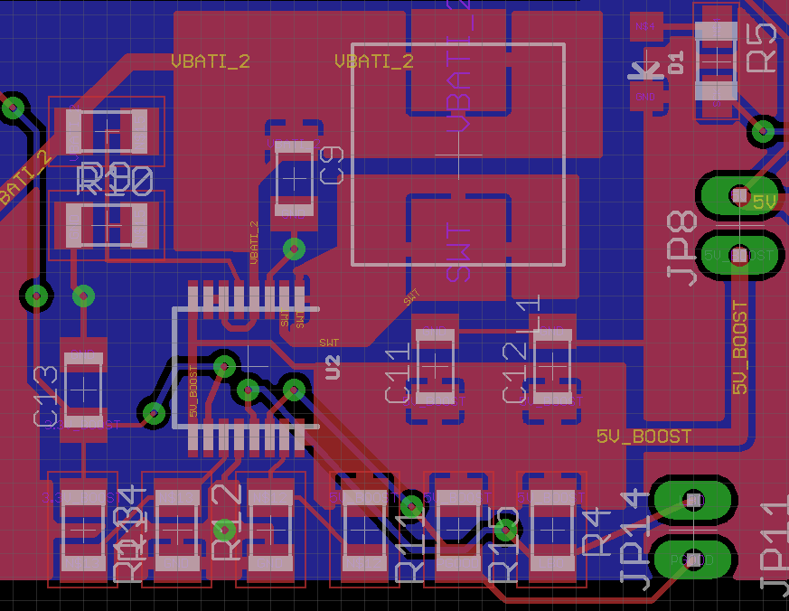
I've got a circuit configured like the diagram below to produce two outputs, 5V and 3.3V:-

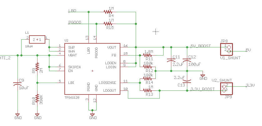
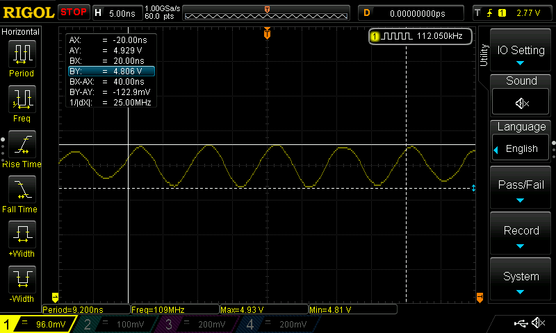
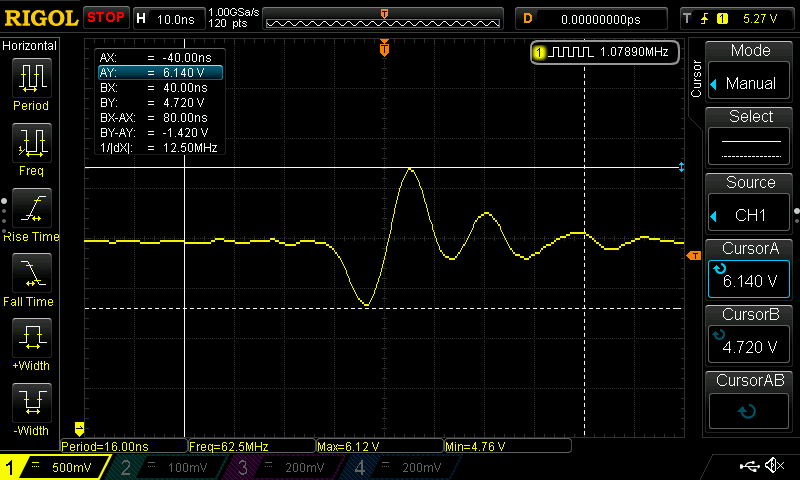
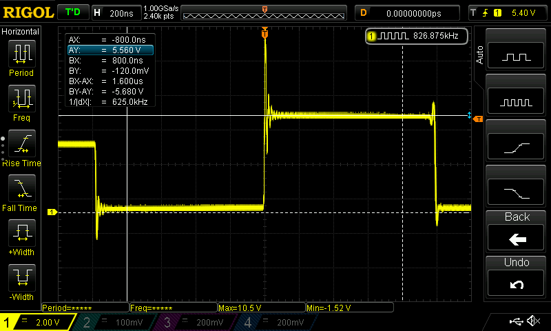
I've noticed that when operational with the shunts removed (i.e. no load attached), the voltage of LDOOut is around 4.8V and Vout is 5.4V.  Have I incorrectly sized the voltage dividers at LDOOUT and VOUT?  The input is a single cell LiPo battery but if I replace it with a bench supply set to 3.7V i get the same result.

  • The feedback resistor for the VOUT is not correct, the setting voltage is 5.5V.
    could you share the layout and the operating waveform of the 5V and 3.3V output, SW pin.
  • Hi Jasper,

    Apologies, I meant to say that output was designed to be 5.5V not 5V.  I've attached a screenshot of the PCB layout:-

    Here is the Vldo waveform:-

    the Vout waveform:-

    and the SWT waveform:-

  • I've also noticed that the resistance between pins 15 (FB) and 16 (VOUT) is approximately 500K. I was expecting a higher resistance between these pins, is this typical for the TPS61120 or indicative of component failure? I've double checked the traces, solder bridges and removed any flux just in case but still the same.
  • the layout is not good. the power routing must be short and strong, especially the connection of COUT and the IC. this is an application note about the layout for boost converter"www.ti.com/.../slva773.pdf". although it is not the same device as TPS61120, the principle to deal with the power routing is the same.
    about the LDO out of regulation problem, is the voltage normal if add some load? i'm thinking maybe is caused by high ripple coupling into the LDO output.
    you can apply an EVM for reference. the EVM can help to rule out the setup or measurement problem.