This thread has been locked.

If you have a related question, please click the "Ask a related question" button in the top right corner. The newly created question will be automatically linked to this question.

TPS54160: TPS54160 Question

Part Number: TPS54160

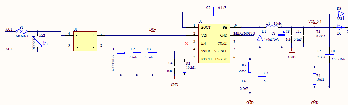
I used TPS54160 design a power supply, input voltage AC12-24V, rectifier filter DC voltage of about 40V (consider the grid voltage fluctuations + 20%), the output voltage of 5.4V, the output current of 0.1-0.3A.


Question 1: The chip of PIN3 with enable and undervoltage lockout function, because the output power range is wide, the divider resistor is not good, in order to simplify the circuit, so the pin is floating, Is this application risky?


Question 2: TPS54160 Switching frequency adjustment to 1.1MHz, inductance L1 election 10uH (power inductor MS127-100MT 5.4A (Isat) -0.0216Ω), filter capacitor selection 470uF electrolytic capacitor and 22uF ceramic capacitors. The Chip PIN4 and PIN8 of the parameters of this election appropriate? Such as the below SCH R3, C7, C6, C4, R2.


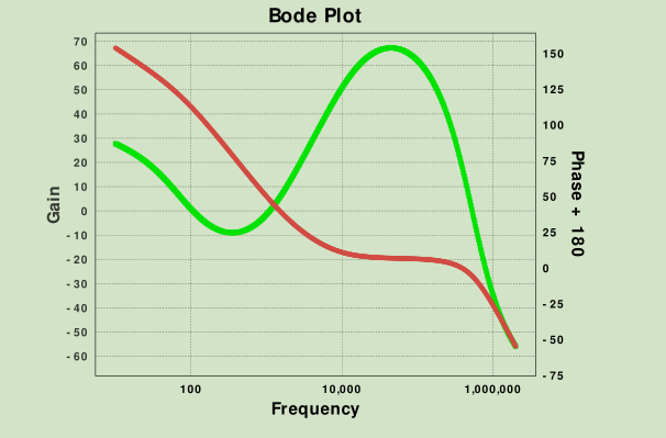
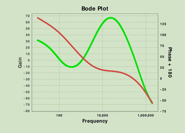
I have three questions about power stability, please help me check it.
1) Is the chip margin greater than 45 °?

2) Is the bandwidth gain less than 110Mhz?

3) Is the gain margin less than -10dB?

  • who can help me to answer about the question, thanks very much~
  • Webench is a good tool to answer these questions. It provides simulations of Bode plot, transient response, etc.

    Please go to the product folder www.ti.com/.../TPS54160
    Use the Webench designer at the lower right hand side of the page to generate your design. You can tune your design by turning the nob at the center. If you prefer higher frequency smaller inductor design, turn the nob to the 'smallest footprint' side. you can also manually change component values after the schematic is generated.
  • Dear Yang:
    I have used Webench the TPS54160 simulations of bode plot, such as the report in the attachment, please help me to check it.
    what the different of the two report about bode plot,

    Whether the circuit designed with these parameters is appropriate

    thanks~

  • Is this design generated by Webench?

    Just from the curves, the crossover frequency is way less than 10kHz, maybe a couple kHz. it is pretty low crossover frequency. The phase margin is around 40 degree, less than 45 degree. The gain margin is decent.

    The compensation should be adjusted such that it crosses 0dB line at higher frequency, ideally around the peak of the phase curve.
  • Dear Yang:

    yes, this is designed by Webench.

    but,I have changed some parameters,and then the emulation report is as follows.

    Please help confirm if there is a problem with this use?

    TPS54160_webench_esim.pdf

  • The reason for low crossover frequency in your design is the 470uF output capacitor. I've run TPS54160 Webench design as well. The recommended Cout was 47uF. And upper limit of Cout is 235uF. Can you reduce the output capactor to 220uF and run the Webench simulation again, if large amount of Cout is preferred.