Hi,
I found this article:
by Brian King and try to follow the schematics.
Unfortunately, it doesn't work as expected.
At small duty cycle values, the gate pulses for my power stage looking well, no Problem:
Signal names were selected according Brians schematic.
The waveform diagram in Brians article isn't correct, cause the positive and negative area of the pulses has to be the same to have sufficiant core reset.
I personally wondering, that the voltage Q2-D isn't rising to Vdd_drive, here about 17V, after the drive is switched off. As Brian describes his circuit and as I understand it, this voltage has to rise to Vdd-drive plus a forward biased Schottky Diode.
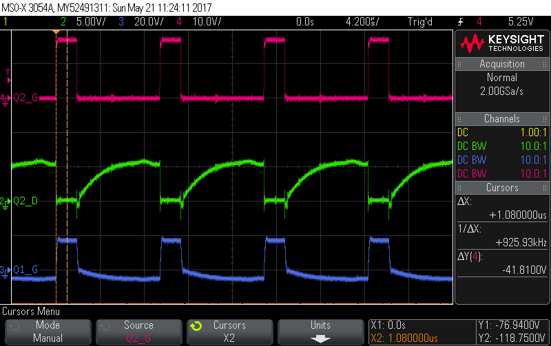
When I use longer duty cycles, some kind of flux walking set in. My core has 56Vµs and my drive voltage is 17V, so 3.2µs should be ok, my Problems starting at 2.4µs, here 3µs pulses were used.
The first cycle in this picture shows the saturated core, indicated by decreasing voltage at the end of the on phase. After switching off, the voltage at Q2_d rised imediately and we see, what Brian stated, so the core is properly reset?
The next cycle Shows the same behaviour as we have seen at smaller duty cycles before, and the next cycle also, but the effect is growing and than the core saturates again and then a cycle like the first follows.
Did flux walking take place?
Why does the circuit reset the core (more or less) only after the core saturates? Whats going on during the other cycles?
I tried to plot the voltage across the primary winding using the 'math' function of my scope:
Ok, the secondary voltage (= gate of my power stage Q1_G) just does what the (calculated) primary voltage do ==> the transformer is ok? The secondary voltage isn't disturbed by some malfunktion. The power stage works fine.
Did anybody have an idea whats going on here?
Thanks for helping.
With best regards
Gerhard


