


Hi
We have for some time been using the LM53601 step down converter (5V out) with a TPS73633 drop-down regulator (3.3V). In between the 5V and the 3.3V supplies we charge a super capacitor which can provide backup supply to safely shut down the load circuitry when the external supply is disconnected. The disadvantage of this method is that the 3.3V output can only be maintained as long as the super capacitor voltage is above 3.6V (the minimum input voltage to the LDO).
We would like to upgrade the circuit to use a buck-boost-converter as illustrated below. We are currently looking the TPS63031 as a potential candidate. The advantage of this is (hopefully) that more of the capacitor energy can be utilized during shutdown.
A simple schematic of the setup is given below:
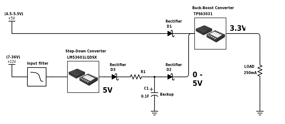
(We do not want to charge the super cap if only the +5V supply is active. If the +12V is connected, the super capacitor shall be charged to secure some backup-energy.)
In normal operation, the load is supplied directly from either the +5V and/or +12V external supplies. We want the normal operation scenario to provide a stable 3.3V output to the load. In this scenario, the 3.3V converter will operate with 5V in and 3.3V out.
When the external supplies are disconnected, the C1 super cap will deliver energy to the 3.3 V converter. Initially, the input voltage will be above 3.3 V and after some time below. According to the datasheet, TPS63031 will be able to deliver a 3.3V output until the input voltage has dropped to approx. 1.8V.
R1 is used to limit the inrush current into C1 (0.3-1.0 ohm ESR).
Questions
- Do you see any obvious problems with suggested circuit?
- Do we need D3 to prevent C1 to discharged backwards through the circuit when the LM53601L input drops to zero?
- The LM53601L is currently driven by the internal clock. Do you recommend synchronizing the clocks of the two converters to reduce EMI/EMC?
- If so, can you recommend a way of doing this?
- In your opinion, will the additional switching power IC drastically worsen the EMI / EMC emissions compared to using LM53601L with the current LDO?
- The +5V line is USB VBUS. Would you be worried about EMI from the buck-boost conterver back into the USB supply?
- If so, can you recommend one of the TI chips for reducing EMI for this purpose?
We highly appriciate any help you can provide.
Thanks.
Br
Christian
