This thread has been locked.

If you have a related question, please click the "Ask a related question" button in the top right corner. The newly created question will be automatically linked to this question.

PMP40025: UCC28730 controller /PWM IC working

Part Number: PMP40025
Other Parts Discussed in Thread: UCC28730

Hi,

    I am working on PMP40025(AC to DC flyback converter) schematics attached , I am trying to fabricate an test the reference design given in TI Website.

    MOSFET in AC DC converter is  controlled by UCC28730 - PSR Flyback controller.


    The Vdd supply pin in UCC28730 can charge internally from rectified high voltage dc input, when it reaches 21 V, the IC is enabled. 

    When 21 V reached, the IC is enabled and a single pulse is observed at start up.

    the controller produces continuous gate signal based( similar) on pulsed Vs input.

     I gave a frequency signal( 3V, 500Hz)  from a micro controller to the Vs input. but only single pulse observed, no continuous gate signal observed.

    How and when it produces continuous gate signal

8154.schematics.pdf     

  • Vaishnavi,

    The schematic you attached is from the TI reference design PMP40025. Can you post your schematic and transformer details?

    Are you testing the UCC28730 in a power supply circuit, or are you trying to test it outside the power supply, in an "open-loop" setup? We need to understand exactly what you are trying to do. It not possible to supply a signal the VS pin from a mico-controller to mimic the real signals that will be seen and measured in a real system. Since the IC has internal closed-loop voltage control, it's not easy to get it into a mode of operation where continuous gate drive pulses are produced - all the correct singals and timings must be present on all the pins, which is very hard to create.

    The IC is best evaluated in a properly-designed closed loop power stage.

    This debug guide for TI's PSR controllers may be useful:
    www.ti.com/.../slua783.pdf

    If you only see a single gate drive pulse after startup, then it may be due to one of the issues discussed in section 2.5 or 2.6 of the above document.

    I hope this helps answer your question. If so, please click the "verify answer" button.

    Thanks,
    Bernard
  • Thanks for the reply and debug guide. will look into this and get back to you.

    I understand the comments.

    Transformer  details:

       RM10 core as mentioned in BOM. Calculated no of windings:

                                Primary: 107 turns

                                Secondary : 15 turns

                                Auxiliary: 5 turns

    Main objective is to implement SMPS for domestic appliances with 48V DC output, 35W output power.

    I was trying to  test the full populated PMP40025 board previously, observed burning of current sensor resistors, R11, R12, & resistor R8. failure of drive transistors Q3 & Q4, & D4 (please refer schematics PMP40025)

    Tried  to debug power supply section and controller. 

    Only after MOSFETS switches, Vs Voltage sense and Cs - current sense can be produced. So tested UCC28730 with internal charging through HV pin.

    Today I tested the AC/DC flyback circuit PMP40025  (with secondary side alone kept open) to check whether the MOSFET is switching.

    1) Gradually increased AC voltage, Vdd of UCC28730 internally charged through HV sense pin, After Vdd reached 21 V volts, (enabling voltage), voltage across Vdd pin starts fluctuating (I assume the controller is activated and starts switching)

        (No external pulse for Vs is given)

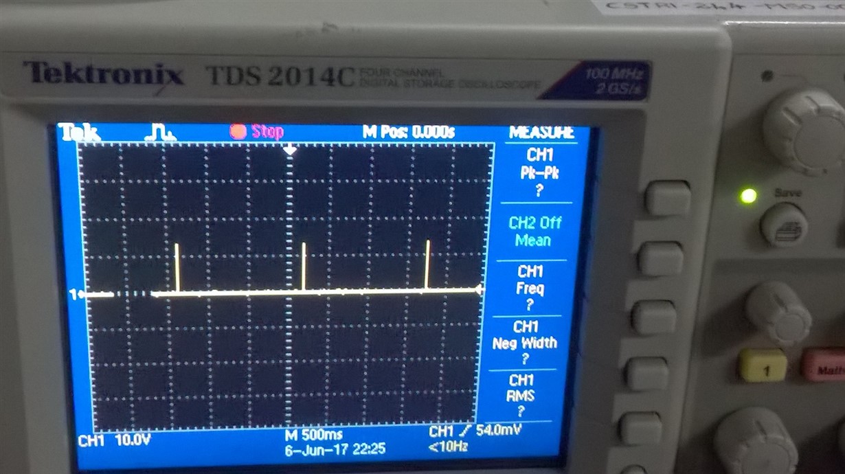
    2) some triggering pulse produced across the DRV pin with  amplitude : 15 V and time period :  4 micro sec, this trigger pulse repeats after 1.5sec ( corresponding image attached)

    3) This same pulse also happens in MOSFETS gate pin. (I feel that this on time is insufficient to drive MOSFET)

    4) Later I increased the AC voltage till 98V, I can see the DC voltage dropped across the MOSFET but it did not switch)

    I assume only after the MOSFET starts to switch, voltage induce in secondary and auxiliary. 

     All the values in schematics are exactly followed.

    Suggest any changes to be done on my side to implement the SMPS.

    Thanks in advance

  • Vaishnavi,

    It's not clear to me, so can you clarify - do you have a board PMP40025 that you got from TI? Or did you make your own board, using PMP40025 as a reference?

    If you made your own board, then clearly there is something wrong or different, so you need to post your own schematic (with values) for review. There is no point in posting PMP40025 schematic, since that is not the exact schematic for your board.

    Your transformer turns ratios are totally different compared to PMP40025, your Np/Ns = 7.13 compared to 1.67 for the reference design - your turns ratio is far too high for 48-V output. What is your primary magnetising inductance?

    You need to double check your transformer design and then follow the debug guide.


    When the UCC28730 reaches 21 V on VDD, it starts up, and generates an initial switching pulse, with minimum peak current demand of 250 mV. If the CS pin does not reach this level within a certain time (4 us for UCC28730) the IC will time out and go into a fault mode, since it could be due to a fault with the CS pin (shorted to GND). Or the input voltage is too low and/or magnetising inductance is too high, so very small current is flowing. The FET will easily turn on is a few hundred ns, unless the gate resistor is very large of the FET has excessive gate capacitance.

    If the CS pin level is reached before the 4-us time-out on the first pulse, then the IC will generate 2 more cycles, and use the info on the VS pin to determine both input voltage and output voltage. If the input voltage is too low, the IC will not generate any further PWM pulses, and will go into fault mode.

    In fault mode, the VDD will slowly decay to a reset level, then the HV pin will recharge VDD to the start level (21 V) and repeat until the fault conditions go away. This cycle timing depends on the size of the VDD cap but is typically 1-2 s. Clearly something like this is happening in your case, and the debug guide above goes through all the possible fault causes and remedies.

    Per the related post by Aravind, if you are seeing issues with components blowing up, there clearly there is major bug in the board or the designs – a short, or reversed component, or some other gross fault.

    Thanks,
    Bernard
  • Sir,

           I replicated the PMP40025 board using respective gerber files and BOM,

           We custom made two transformers

                               T1  - similar to the one mentioned in Reference design.

                                        Primary Inductance : 165uH

                                        Primary to secondary turns ratio = 1.67:1

                                        Primary to auxiliary turns ratio = 5 :1

                               T2  - As we use 230V ac here, I calculated the ratio based on that voltage whose turns ratio i mentioned in previous mail

                                         Primary Inductane = 8 mH

         Curently I am testing with T1 only, and given the calculations and observations for that.

                             With reference to debug guide, section 2.5.1

                                         turn on time ton = (Lpri * I pri)/Vblk

                                                                            = (165 uH * 1A)/(120 V)     [ assumed Ipri peak as 1A, Vblk=85*1.414]

                                                                            = 1.37 us

                                      This ton is less than the desired ton, which satisfies the condition for first cycle.

                            Tested With transformer T1, but secondary side kept open

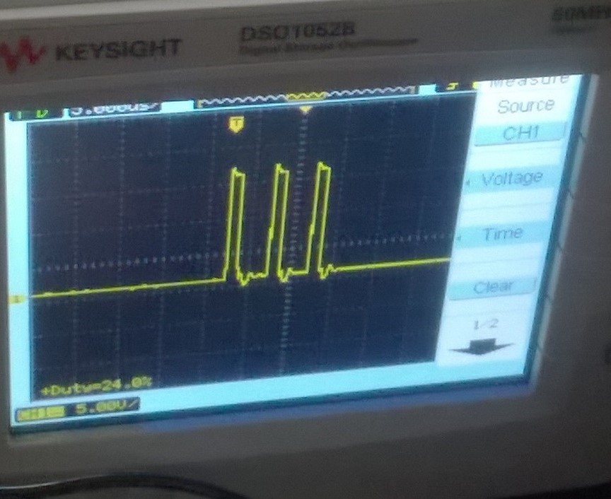
                                      Gradually increased voltage, initially controller went to charge-discharge mode, After 85Vac a set of three pulses produced . 

                                      No pulses observed after two set of pulse

                           Debugging 

                                      Few devices on auxiliary circuit side failed: (with reference to PMP40025 schematics)

                                                     Q3 - short, D5 - short, R7 - 2ohm  - open ,

                                      I feel controller might also be failed, suggest conditions to test controller 

                                      Again gradually increased voltage from zero, but Vdd didnt increase beyond 12.05 voltage

       
    I suppose some over voltage for the cause of failure. Suggest your ideas and comments on the picture and cause of  the failure, so that I will rectify it                    


  • Hello Sir,
    I have changed the transformer winding ratio based on calculations given in UCC27830, and now the primary magnetising inductance is 570uH. The converter output voltage : 52V
    Supplies MAx : 60W at 45ohm resistive load
    Beyond 60W, it goes into start stop mode, and the converter output voltage os zero.
    I would like to check whether current limit mode can be implemented so that it supplies max constant power.
  • Hi Vaishnavi, the current limit on the UCC28730 is implemented as a constant output current limit as you have said. It is not possible to change it to a constant power limit.
    Sorry.
    Thanks.
    Billy
  • Please explain constant output current limit with respect to variation of load.
  • See section 7.3.3 of the datasheet. Beyond a the current limit point increasing the load results in the output voltage falling rather than more current being supplied.

    If the load is in Constant current mode too, the output is likely to collapse or hiccup.

    Regards

    Billy