This thread has been locked.

If you have a related question, please click the "Ask a related question" button in the top right corner. The newly created question will be automatically linked to this question.

LM5576: IC failure

Part Number: LM5576

Hi,  we are using LM5576 Buck converter in one of our product.

Input for the LM5576 is from a battery bank around 60Vin and output is 12V , 0.3A output.

Switching frequency is 71KHz.

Now we face more nunmber of  IC failure from the field at different conditions like sudden power on , either the input side of the IC got burnt and another type of failure is short at the output side across the switching Diode B/W pins 15,16 & 17,18. once we replace failure IC with new one some Boards are working fine, in some cases again the IC fails.

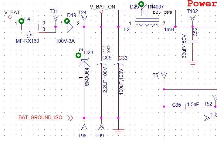
Herewith i attached the Design for reference also can you please propose a suitable LC filter and TVS configuration for our application.

Thanks in advance.. 

  • Can you probe the input voltage, SW pin voltage and Vout waveforms? It sounds like instability damaged the IC. Can you compare your design with Webench design? The input filter L is 3.3mH or uH?
  • I was reviewing this open thread and thought I would chime in. Yang is correct in questioning the value of L2 at 3.3mH. the LC network formed by L2 and C62 can ring up highto 2x Vbatt  if the product is hot connected to the Vbat power source. Since there is a 64V tranzorb in front, there is a great possibility Vin will exceed the 75V rating at the IC. There are several modifications. Place a resistor across L2 to reduce the Q and lessen the ring or add an additional MOV at VIn of the IC,

  • Hi,

    Thanks for your reply.

    Inductor value is 3.3mH.

    i probed the Vin and vout waveforms. i find a ringing voltage around 66V when we enable the SD pin. actual input from the battery is only 51V.

    when i increased the capacitance value the ringing was reduce to some extent.

    now we planed to reduce the inductor value to 1mH and capacitor to 33uf.

    increased the C33 capacitor value to 100uF and placed a freewheeling diode across the inductor.

    please share your opinion on this.

    Thanks in advance.

  • Hi Alan,
    Thank you for your suggestion. I have few queries with respect to your reply.
    1.       Why will Vin might go up to 2xVbat when the battery is hot connected or hot plugged? When the supply is hot connected then the inductor, will it not suppress the sudden inrush of current? Please explain the reason. What is the physics behind in Vbat reaching 2 times its value?
    2.       Transzorb is used to limit the voltage but your statement is again contradictory to me. How come having 64V transzorb will make Vin to see 75V or greater? I agree that transzorb is connected at the input of L2 but still having 64V transzorb at the input of L2 how will that influence in making the voltage go beyond 75V at Vin pin of IC?
    3.       You suggested to use resistor in parallel with L2. Shall I add an RC instead of only one resistor? Say the resistance R = 20 ohm and C = 47uF?
    All my above queries are considering L2 value = 3.3mH.

    Regards
    Omprakash
  • The mechanism for the midpoint voltage of a series R-C ringing up to 2X Vin comes from elementary circuit analysis. Circuit analysis text books such as the classic by S. Ivar Pearson and George J. Maler, or one of the many others will detail the effect. There are certainly newer texts that are written to be studied with access to a simulator. (Pearson and Maler had us submit our simulation decks on 80 column Hollerith cards, the resulting output arriving hours later on fan-fold paper from an impact line printer.)

    Nowadays the effect is easily simulated in a few seconds, the ring-out duration depending on the parasitic ESR of the 10uF capacitor and 3.3mH inductor.

    Actuating the SD control line is very different than hot connecting the circuit to the battery. It is the hot connect event where the initial condition of the input capacitor is zero and the resonant LC will ring up substantially higher than Vin. The input capacitor is already charged if you are just toggling the SD control.

    The use of the clamp diode across the filter inductor would had no be evaluated to make sure the ac voltage across the inductor never exceeds 300mV where the diode would start conducting. 1N4007 is a very slow 1KV 1A silicon diode but this isn't a switching application where switching speed or recovery speed is important. 1N4007 is low cost and widely available for certain. Remember that in the ideal case there is no dc drop across the inductor so placing a resistor across it does not waste power but does reduce the Q of the LC.