This thread has been locked.

If you have a related question, please click the "Ask a related question" button in the top right corner. The newly created question will be automatically linked to this question.

CSD19534Q5A: Footprint mismatch on Recommended PCB Pattern SON 5x6

Part Number: CSD19534Q5A
Other Parts Discussed in Thread: CSD18510Q5B

Hello,

I'm making the footprint for this MOSFET to include it in my design, but looking at the PCB Pattern, I get different measurements on it's pad height.

Using the higher tolerance boundaries:

F11=F3=4.56

F3=4*F4+3*F5=4*0.7+3*0.67= 4.81

4.81 is totally different than 4.56

Nevertheless, using the lower tolerance boundaries:

F11=F3=4.46

F3=4*F4+3*F5=4*0.65+3*0.62= 4.46 this measurement matches.

I'm confused, should I calculate the average between these two?

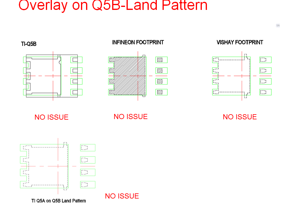
I'm also trying to adapt this footprint so I can use PG-TDSON-8 on the same footprint for alterns like BSC117N08NS5ATMA1

Thanks in advance.

  • Mario,
    What we are saying here is the individual variation of all the pin tolerances is greater than the max variation for the F11 dimensions. In other words, if on pin is a little larger, one of the other dimensions will necessarily be smaller such that F11 max will still be <=4.56. Does that make sense?

    I'll ask our packaging engineer if he has any advice on adopting to Infineon's footprint.
  •  So we would actually recommend using our Q5B footprint, which is just a little bigger, as a universal footprint for our Q5A devices and Infineon 5x6 package.

    So you could look at the CSD18510Q5B datasheet for instance, and refer to the recommended PCB drawing there.