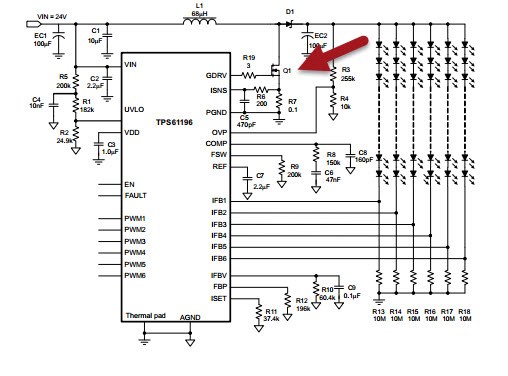
Hey guys,
My switching FET gets incredibly hot and my heat sink has to be massive which makes me think I've done something wrong.
Is it the nature of this architecture? All the heat is in the FET (STP70N10F4 has RdsON 0.0195ohm at 60A). I see the duty cycle is around 75% (measured at GDRV) which matches the equation used to size up your output cap. I understand that this means I have my power supply sourcing current that gets shunted to ground for this time period (can you confirm?). I can increase my Vin voltage to help out(go from 12 to 24V). I was wondering if there was other design tweaking that could be done or common tricks you might be aware of or other? I have 2 designs I’m using this on. One is 10W and everything is nice and cool. My 50W design needs a massive heat sink on the FET. Both designs optimize routing planes and make other considerations for the power paths. Both designs are stable and switch consistently. My R7 has been sized a little above the I(Ldc)+I(Lpp). Thanks for any comments.
Thanks!


