This thread has been locked.

If you have a related question, please click the "Ask a related question" button in the top right corner. The newly created question will be automatically linked to this question.

TPS40170: Problem with stable working (and working at all)

Part Number: TPS40170

Hello

I have a big problem to make DC converter to work.

Schematic:

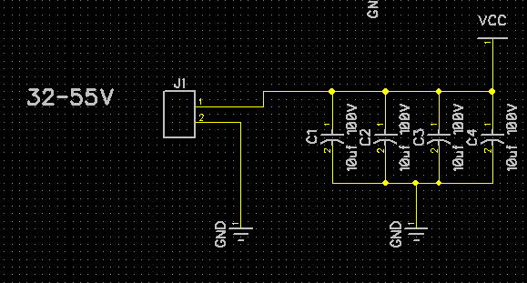
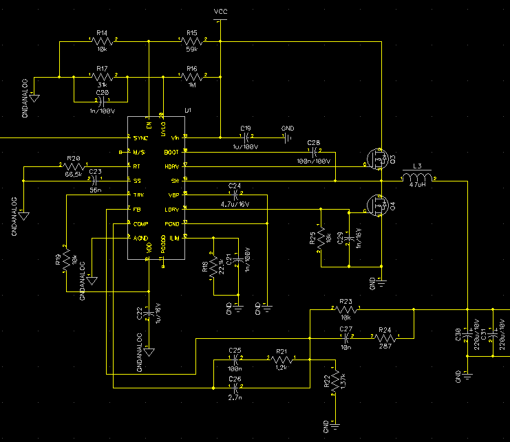
Its based on Webench Designer project.

Main assumptions:

32-55V input voltage

5V @ 4-6A current

f=120kHz

Soft start 5-6ms (BTW. there must be a bug in Webench in calculating capacitor value for softstart, if I set any time, the result is always 2,2nF for SS Cap)

PCB Layout (2 layer):

Top:

Bottom:

After building prototype the first power up (40V Vin) was only 1,7V on the output.

I removed UVLO and bypassing it from Vdd (for testing at lower input voltage).

At about 8V to 13V i got a 5V on output but after incresing Vin at about 21V something happened (current limiter ?) and output drops to 1,7V. Now i cant get 5V at any Vin.

What i tested:

- different frequencies (100, 200, 300 kHz)

- longer soft start

- different Ilim resistor values

No way, it can't working.
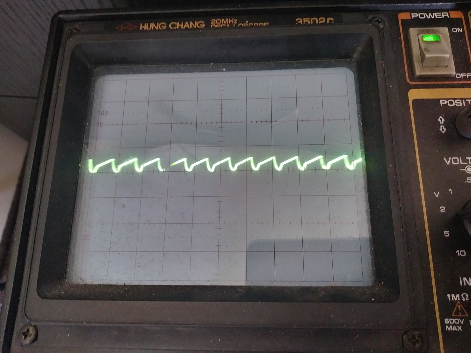
Here some o'scopes:

2V/DIV in all screens

SS pin from 4,5 - 28V

SS pin (Vin 29V and more):

High side Gate pin:

Low side Gate pin:

Somebody can help with this magic ?

  • On the schematic, some of the components are connected to analog ground, as well as the AGND of the IC. Some signals refer to GND, as well as PGND pin. All the control input signal to the IC should be referring to AGND, such as FB divider, Comp network, Ilim. Gate driver related signals should refer to GND. From the schematic and layout shown, it is hard for me to see how AGND and GND are tied together. They should be tied together at a single point through a net tie.

    The layout can introduce noise to the control components as well. The C1-C4 Vcc bypass capacitors should focus on bypassing from the drain of Q3 to the source of Q4. Since there's no internal ground layers as shielding, top and bottom layer signals can couple switching noises easily.

    For the waveforms, what is the scale of SS pin voltage? What is the min and max voltage of the SS pin voltage? If the min voltage is above 0.6V, it should not affect the operation of the controller. If the min voltage is below 0.6V, it may override FB voltage. Then we need to figure out why it is discharged to below 0.6V.

    Please carefully probe the FB pin voltage, it should be at 0.6V. If it is below 0.6V, it could be because of SS pin voltage too low, or HS drive signal should be high most of the time.

    Is the HS drive and LS drive signals have the same time scale and voltage scale?

    Please probe Vin, SW, and Vout as well.
  • Thanks for reply.

    AGND with PGND is connected by R26 0Ohm resistor in a single point.

    Are you sure about Ilim circuit to AGND ? In datasheet (page 3) Ilim is refered to PGND.

    On o'scopes signals there is 2V/DIV on all, time reference is different.

    Thanks for tips. Let you know about measured values.

  • Please follow the datasheet in that case.