This thread has been locked.

If you have a related question, please click the "Ask a related question" button in the top right corner. The newly created question will be automatically linked to this question.

TPS92515HVEVM-749: Simulation Vs. Implementation

Part Number: TPS92515HVEVM-749

Greetings!

I have been evaluating the TPS92515HVEVM-749. I modified the circuit to do Shunt PWM and analog dimming accordingly to datasheet (put diode, resistor, and pot). However, when I did the shunt FET, I could see the oscillation at the very first when signal is being turned on. I thought that I did not charged the coff properly by choosing the recommended value for R_off2 according to the EVM datasheet which is 309k. In this test, I put an external NFET with 0.25mOhm Rds(on) and do the calculation to find the correct R_off2.

Should I put a snubber circuit? Populate (R8 and C10)

Experiment Setup:

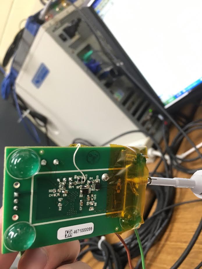
 Please see the picture that I uploaded:

Thanks,

Yo Shua

  • Hello Yo,

    I'm guessing you are showing me the edge of the shunt FET PWM LED voltage? How about the LED current? That would be the important spec and may not ring the same as the voltage. The timebase seems to suggest that. In any case a couple of comments for you:

    1. The snubber you mention is across the rectifier diode. Those footprints were put there in case the switch node needed to be snubbed to pass certain EMI requirements. If you are talking about ringing on the output voltage and/or current it will not do much. If you need to get rid of either for some reason you would need an RC snubber across the output tuned for the parasitics of your particular load.

    2. Calculating Roff2 can be a little tricky, it will only get you close. You will want to put a current probe on a loop of wire in series with the inductor and tune Roff2 until the peak-to-peak inductor current ripple is the same with the FET off as it is with the FET on. It usually needs a little tweaking due to tolerances.

    Shunt FET dimming is very high performance but usually takes a little bit of bench work to optimize.

    Regards,

    Clint

  • So, I tried to use whatever I have in my bench. I use multimeter's shunt resistor to measure its current (I know it's a bad setup), but I just want to see what its waveform look like. Since the multimeter's shunt was placed on the +, I try to probe its differential voltage.

    and I got this result: (black: out current, brown: out voltage)

    I can still see that much ringing and the current does not behaves correctly (I assumpt that I should put the Rsense on the (-) side). To have better understanding, should I use the current probe? Also, what are the next step to improve the ringing? Is this normal? Also, I am afraid that Its voltage can damage the internal NFET (max DRN-SW is 65V.

    Best Regards,

    Yo Shua

  • Hello Yo,

    A current probe with a very short loop of wire is the best. But yes, the ringing is real. It is caused by the parasitic inductance between the shunt FET and the LED and if the simulation includes any parasitics it will show this.

    When you shunt FET dim you can get rid of the majority of the ringing by placing the shunt FET directly next to the LEDs to minimize the parasitic inductance. If this is not possible and/or doesn't reduce the ringing enough then you will need to place an RC snubber across the shunt FET as I mentioned. It will need to be tuned for your particular load and you can dramatically improve the ringing with one.

    As for damage, depending on the inductor characteristics (if it has a low SRF) the spikes may be seen at DRN-SW, but likely reduced. But usually damaging the device is less of a concern than damaging the shunt FET.

    Regards,

    Clint