This thread has been locked.

If you have a related question, please click the "Ask a related question" button in the top right corner. The newly created question will be automatically linked to this question.

TPS65912: Unused enable pins.

Part Number: TPS65912

Hi,

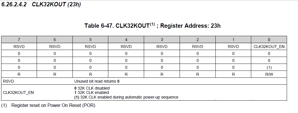
I can't find the schematic checklist for TPS65912x. Does it correspond to the one provided for TPS65911x? I don't intend to use EN2,3,4 so can I just leave them floating? Also, does the register bit CLK32OUT_EN need to be set to 1 for power up? What if it is disabled, would the PMIC still power up as expected?

One more question, can the registers be reprogrammed during OFF state or only during active?

Thank you

  • Hi,

    I have forwarded this E2E to the responsible Applications Engineer and we will get back to you as soon as possible.

    Thanks.

    Murthy
  • Hi,

    You can leave EN2, EN3, and EN4 floating. The registers for these should be set to 0x00 to disable them.

    In the data sheet, the CLK32KOUT register is defined as shown:

    This suggests that the default is 0, however there is a note that the clock is enabled during the automatic power-up sequence.

    To reprogram the registers, the device needs to be on. Once the device is completely off, the registers will boot back to their default values. However, you can enter a sleep mode, where the registers do not loose their programmed settings.

    Thanks,

    Nastasha

  • Thank you for your response.

    I was wondering if you could help me with a couple more questions:

    1) I'm finding some inconsistencies with the output default values and their respective bit strings. For instance,

    LDO1_OP - according to table 4-2, we should expect an output of 1.7V . When I look at its default bit strings, SEL[5:0] for CONFIG1 LOW, I see 001100, which translates to 1.1V as shown in table 6-43. Such discrepancies appear as well on LDOx_OP/AVS, LDO6, 8 and 10. Fair to say there are some typos on the register bits? Or are the typos on table 4-2?

    2) Say I want to work with LDO1_OP and I set its corresponded register bit at EN1_SET1 to 0. I don't understand how I would be able to enable or disable LDO1_OP, is the only option set LDO1_EN1 to 1 and hardwire pin EN1?

    3) I would appreciate if you could also clarify the difference between setting an enable bit register to (1) and just 1 (as an example, look at table 6-27).


    I appreciate your attention and look forward to hearing from you soon.

  • Hi,

    I have reviewed the datasheet and understand the inconsistencies you are referring to. I will am going to look further into these questions and get back to you shortly.

    Thank you in advance for your patience.

    Best,
    Nastasha
  • Were you able to find the answers to my questions?

    Thank you

  • Hi,

    We apologize for the delay, the office was closed yesterday for holiday. Please use table 4-2 as your reference for startup voltages.

    Also, if EN_SET1 is set to 0, then yes, you would have to use the LDO1_ENABLE bit in the LDO1_AVS register to turn on the LDO.

    Thanks,
    Nastasha
  • But I'm asking about LDO1_OP, though. How do I enable or disable it? Is the resource meant to be constantly ON if the OP register is chosen?!

  • You can enable LDO1_OP using the LDO1_AVS register or the EN_SET1 register. If you use EN_SET1, you would need to supply power to the correct enable pin. For more information on this, you can also refer to our datasheet. Table 6.60 describes how the enable pins can be configured.