This thread has been locked.

If you have a related question, please click the "Ask a related question" button in the top right corner. The newly created question will be automatically linked to this question.

TPS65131: Negative rail discontinuous

Part Number: TPS65131

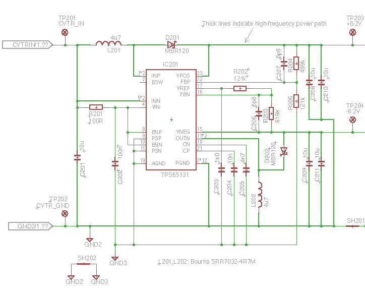
I have a 3.7V to +/-6.2V converter using a TPS65131. The circuit is essentially the same as the TPS65131EVM, with R2=121k, R5=619k, 6.8pF in || with R5.  CN is 4.7nF to AGND.  Vref has 1.0uF to AGND.  Circuit layout is as tight as I can make it with 0603 components, on a double layer board with ground and power traces using polygons as large as possible, as much like the recommended layout as I could achieve with 0603. PSP and PSN are connected to AGND.

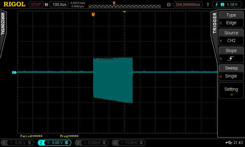
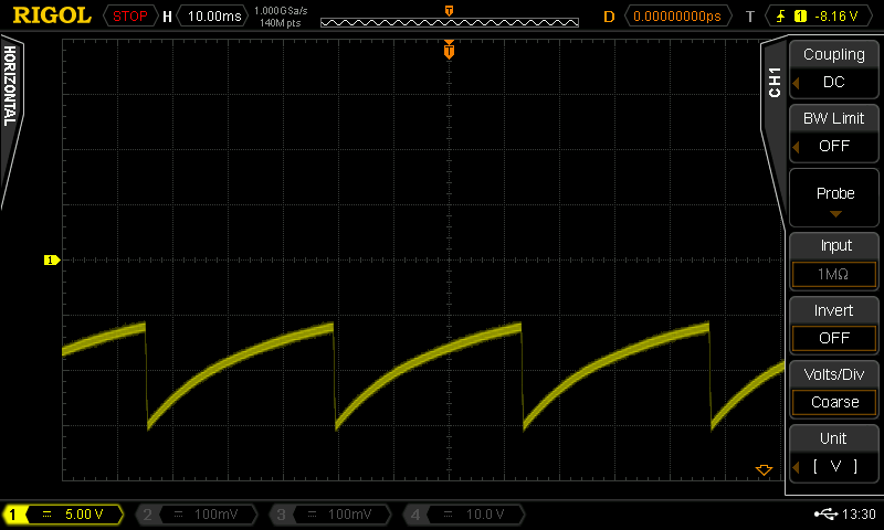
Positive rail works perfectly.  At no load, negative rail works fine with 2.5V input, but with anything higher, it goes into a discontinuous bursty mode where every ~80msec it does about 250usec of ~1.4MHz rectangle wave, with the negative excursion increasing over the 250usec interval till it gets to about -10V.

The EVM with the same component values works fine; but both of my two prototype boards fail in the same way as each other.  So I am assuming this is a problem with my PCB layout.  But, what should I look at?  Are there any experiments I can do to try to track this down?

Here's what the burst looks like:

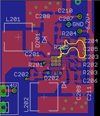
And here's the relevant part of the board layout:

  • Hello Walter,

    Can you as well show a scope plot with the voltage of the CN-pin? Did you try to disable the booster, how does the inverting stage behave, still the same?

    I noticed that the AGND is not connected to the power pad of the IC, this is quite critical. Add a polygon (yellow marked) on the top layer and connect the AGND pin to the power pad of the IC on top layer as well. You can move C205 (an all other caps/resistors below) further down. 

    Thank you.

    Best Regards.

    Ilona

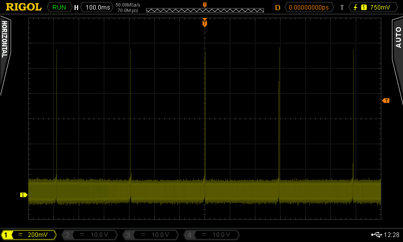
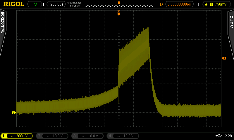
  • Thanks for responding, Ilona!  Here are views of CN at 100msec/div, 200usec/div, and 200nsec/div.

    Regarding the layout, it's a bit hard to see but AGND is definitely connected to the power pads.  Here's a better view.  

    Note the overlapping vias indicated by the yellow arrow.  It's hard, in Eagle CAD, to intentionally connect polygons from different signals... still, maybe I need to do a better job of this.  I wanted to connect AGND at only one place but maybe I need a lower-impedance connection?

    Here's what it looks like on the schematic (the overlapping vias are component SH202):

    Thanks again for your help!  I would love to get this project into production, I've got hundreds of customers waiting for it :-(

  • To answer your other question: I haven't tried disabling the positive converter; I can't do that without physically cutting traces. If it would help a lot with the troubleshooting, I can do it, though.

    By the way, at high loads (>40mA) the negative converter finally becomes continuous.  I need it to operate with no audio-frequency noise down to about 5mA, though.

    I'm noticing the negative regulator is also badly out of regulation.  According to the design it should be -6.2V, and I have measured the resistors to make sure they match the schematic (e.g. I didn't accidentally pick from the wrong reel).  At high loads where conversion is continuous, Vneg is a steady -20V (!!); at lower loads, it is a sawtooth that never gets less negative than the nominal -6.2V, but that gets much more negative.  See below at 10k load; it is sawtoothing from -6.2V to -15V, with a period of about 33msec.

    Should CN and CP be referenced to DGND, rather than AGND?  Am I getting current noise from the charge/discharge current through C204/C25 coupled into the Vref pin via C203, maybe?

  • Hello Walter,

    Thanks for the detailed information.
    CN-Pin behavior looks normal, so nothing obvious on the actual regulation loop.
    Regarding the layout, you are absolutely correct in connecting AGND at only one place but we also recommend to make this connection between the AGND pin and the thermal pad directly (same as you did with PGND pins and the thermal pad). This is the lowest impedance connection.
    Due to the scope plot of VNEG this seems not be relevant anymore. How fast do you ramp up the supply voltage?

    Best Regards,
    Ilona
  • I'll tweak the next iteration of the board to connect the AGND pin directly to the thermal pad.  It sounds from what you say that is not likely the cause of the present issue, though.

    In the actual application it ramps up more or less instantaneously, i.e., a MOSFET is turned on and thus the battery is connected to the input of the converters.  On the lab bench, I can ramp it up slowly.  Informally, I think I've tried that just by happenstance and I don't recall it changing the behavior at all, but I will try it more systematically today.

    Is there anything else I can check at the same time?

    Thanks,

    Walter

  • Hello Walter,

    Sorry for the delay. Did you already check a slower ramp?
    What you can try is to use a ferrite bead (100Ohm@1MHz) instead of the RC filter on VIN. We have seen that a fast ramp (< 15µs) of the input voltage can cause misbehavior on the IC, but usually this does not happen in a typical application.

    Best Regards.
    Ilona
  • I tried ramping up slowly, and it made no difference.  However, I think I might be on to something.  In the below, the yellow trace is Vneg; at zero load, it is sawtoothing between -6.2V and -15V.  But the blue is Vref.  Note the big spikes there, nearly 700mV.

    Now, here's a view of what happens during that spike:

    Here's what I think is going on.  The voltage is too negative, so nothing's happening and the capacitor is gradually discharging.  It finally gets to -6.2V, at which time the converter says "oh, I better start making some juice."  It does so - but in so doing, the conversion noise couples into Vref, shifting it more positive, so rather than just charging a little bit and stopping again, it keeps going, up until such time as Vneg is so negative that it outweighs even the shifted-positive Vref, and conversion stops again.  At that point, of course, the noise goes back to normal so there's nothing to make it start converting again until it finally sags back down to 6.2V and the cycle begins again.

    So the question is: why is there noise on Vref?  After all, that's part of what the grounding scheme is supposed to prevent.

    Should Vref be bypassed to the same ground node that CN is tied to?  Or to put it differently - should CN be tied to the same ground node that the inductor is?  As you can see in the above schematic, right now I've got the inductor going to PGND and CN going to AGND.  Is that a mistake?

    Thanks!

  • Following up on my own question after a bit more thought & reading: No, CN and CP are compensation caps, they should indeed be connected to AGND, not PGND.  I think my schematic (posted above) is correct with regard to where the high frequency power path is.

    But I do think this is about conversion noise coupling to Vref somehow.

  • I think I figured it out! I removed the 6.8pF feedforward capacitor and now I have continuous operation, with steady output voltage, even with no load.

    Next I'll try putting a resistor in series with the 6.8pF to see if I can split the difference between load response time and noise injection. That is one of the differences between my circuit and the EVM - it has a 51k resistor in series with the 6.8pF.
  • 6.8pF in series with 100k works fine. I didn't try other values because I didn't have any better values handy in 0603 format.

    I'm super happy!