This thread has been locked.

If you have a related question, please click the "Ask a related question" button in the top right corner. The newly created question will be automatically linked to this question.

UCD3138A: problem with a huge offset

Other Parts Discussed in Thread: UCD3138A, UCD3138A64OEVM-662, UCD3138A64

Dear TI,

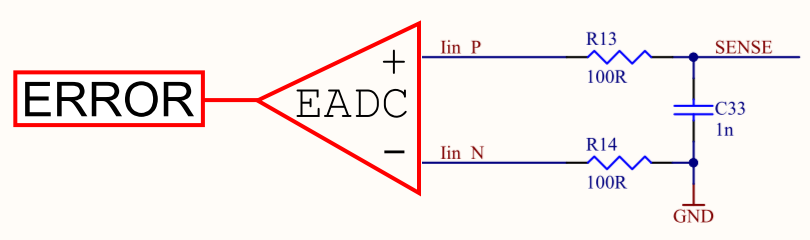
I'm developing firmware for a device based on UCD3138A. The device regulates current, so it measures voltage on a current sense resistor by means of front-end 0 (EAP0-EAN0). The current sense resistor is on low-side, so one of its terminals is connected to ground, along with EAN0.

The problem that occurs in this case is that the device behaves exactly like the current sense resistor was connected to a negative voltage instead of ground (to which it is connected).

When DAC_VALUE is set to 0, the control loop produces some high-side PWM pulses, which cause some current to flow through the load. The voltage measured on the current sense resistor is far higher (like 40x) than any voltage that would correspond to output equal to 0 of the EADC. The same voltage is applied to the input of the front-end. However, the error value reported by the device is 0, and in this state the output value of the filter is non-zero (only the integral branch is active, with KI = 1, branches P and D have their K coefficients set to 0 and are explicitly turned off in control register). The output value of the filter seems to match the observed duty cycle. When the supply voltage is varied, the duty cycle changes accordingly and the output current is kept regulated at the same (invalid) non-zero value. This means, that EADC is able to produce negative error signal to decrease the integrated filter value - but it doesn't drive that value to 0, as it should, maintaining the (invalid) regulation instead, and the error signal becomes 0 despite of high non-zero feedback. This feedback is of the order of 10mV, which should give the error value of about -10. EADC is configured in automatic gain shift mode, but it has been also tested with constant 8x gain (AFE_GAIN = 3).

Two prototypes were tested and both experience this behaviour, but with different "minimum duty cycle" - i.e. for example one device doesn't go below 15%, and the second below 10% (for the same supply voltage).

For higher output settings the devices regulate the output correctly (at least: without such unexplainable effects).

Please, help me debug the thing. What else can be checked? Are the any specific details not described in documentation?

Best regards,
Adam

  • Hi, Adam,

    Can you calibrate the EADC offset if it is the case? If it is possible offset, add some external offset to pull output signal above zero.

    Regards,
    Sean

  • Hi Sean,

    can you confirm that UCD3138A in fact suffers from such a huge offset?
    According to datasheet, the offset should not exceed +/-4 LSB of EADC, meaning +/-4 mV if I understand correctly. Is that so, or do I read this documentation incorrectly?

    How do you calibrate offset in UCD3138A?

    I have also checked the operation using UCD3138A64OEVM-662 eval module. I've connected the output of high-side PWM to RC filter populated on the board (jumper J33, pins 0A-FLTR), then its output through jumpers J38 and J37, so this also goes through a potentiometer. In this case with DAC_VALUE set to 0 I still measure 8.2mV (but my multimeter may not be the most precise one), however, a significant difference to the said design using UCD3138A, the integrated filter value gets down to 0, and the PWM action stops. Even more, the EADC produces negative error, and the integrator value becomes -8, so the loop does react to the offset, but is unable to decrease the already zero PWM duty cycle. I think that in this case the offset has to be caused externally.

    Can there be any significant difference in how UCD3138A is configured?

    In the said UCD3138A-based design if you turn off the PWM action the produced current drops to zero, so the circuit itself apparently is able to behave the correct way.

    Best regards,

    Adam

  • Hi, Adam,

    I don't think EADC has a huge offset. To verify the offset, you just need turn off power stage, and supply bias to UCD3138A. Then you can apply DC voltage to EAP pin (assuming EAN is grounded). Read XN output. You can average out XN to reduce any noise affect. UCD3138A don't have much difference from UCD3138A64.
    If EAP is negative, I am not sure how much offset is introduced.

    Regards,
    Sean
  • Hello Sean,

    here we deduce the offset based on what we read on EAP-EAN with a meter when the control loop provides stable voltage and the internal error value (EADC value) reads 0.

    In this case UCD3138A controls two FETs for synchronous rectification. If the high-side FET is forced to be permanently off, the output drops to 0, so this part looks OK.
    (Without forcing the off state of the high-side FET the control loop produces a non-zero output and "ignores" a significant offset, as I reported in the first message.)

    The feedback signal in the device develops on a low-side current sense resistor (which is connected to ground) and is then fed to EAP, with EAN connected to ground. Are there any additional requirements/precautions/considerations for using the EADC this way? Does it need any additional input resistance? Does it source or sink current?

    Best regards,
    Adam

  • Hello, Adam,

    Don't use large input resistor , typically less than 1k. Are you measuring low side switching current or output average current? I guess there is no current amplifier either.
    Use my last email to verify the offset without power stage running.
    Regards,
    Sean
  • Hi Sean,

    we're measuring average output current. We drive two FETs forming a synchronous converter with an LC tank. The sensing circuit looks like this:

    SENSE is voltage developed on current sense resistor, 22mOhm in this case. We've tried also with R13 and R14 replaced by zero-Ohm jumpers, nothing changed, so this suggests that we're not experiencing problems related to any current flowing to/from EADC inputs. According to documentation the input offset is limited to 5uA anyway, so we'd have an additional 0.5mV in worst case conditions.

    Should we have a resistor from Iin_P to GND? Or between Iin_P and Iin_N? Documentation doesn't say anything like that would be necessary.

    Best regards,
    Adam

  • Adam,

    I guess the voltage on SENSE point is negative, right?

    There is no requirement to have a resistor between Iin_P and Iin_N. But it is preferred to move the C33 on the left side of R13.
    5uA doesn't cause large offset in your circuit.

    Regards,
    Sean
  • No, the SENSE voltage is positive.
    Best regards,
    Adam