This thread has been locked.

If you have a related question, please click the "Ask a related question" button in the top right corner. The newly created question will be automatically linked to this question.

BQ25703A: The output ripple is big

Part Number: BQ25703A
Other Parts Discussed in Thread: BQ25703

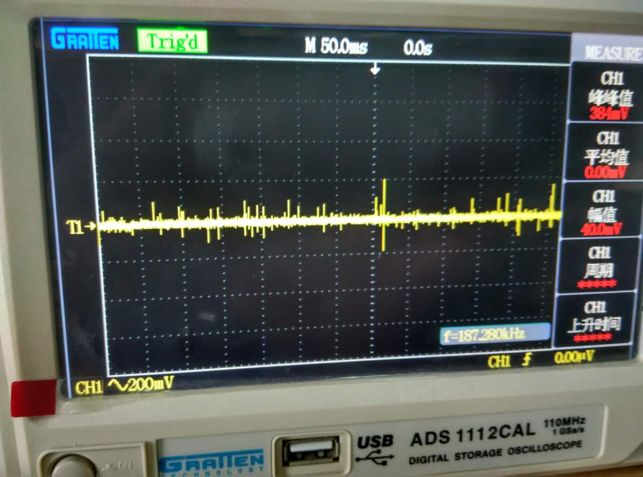
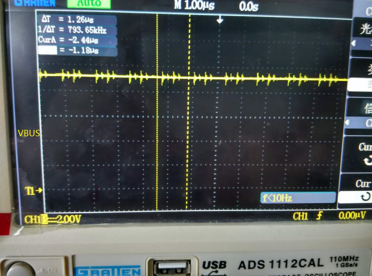
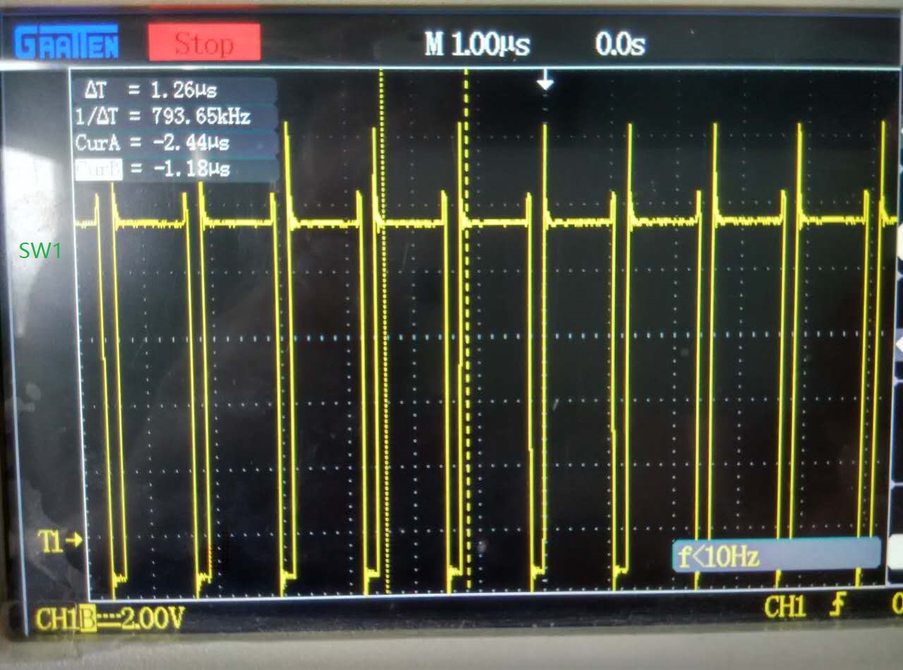
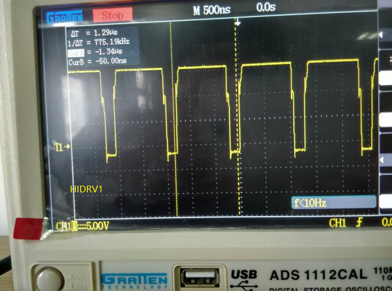
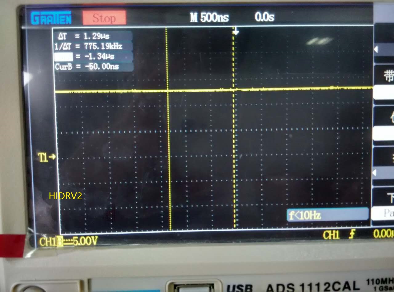
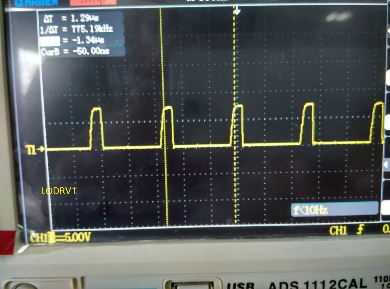
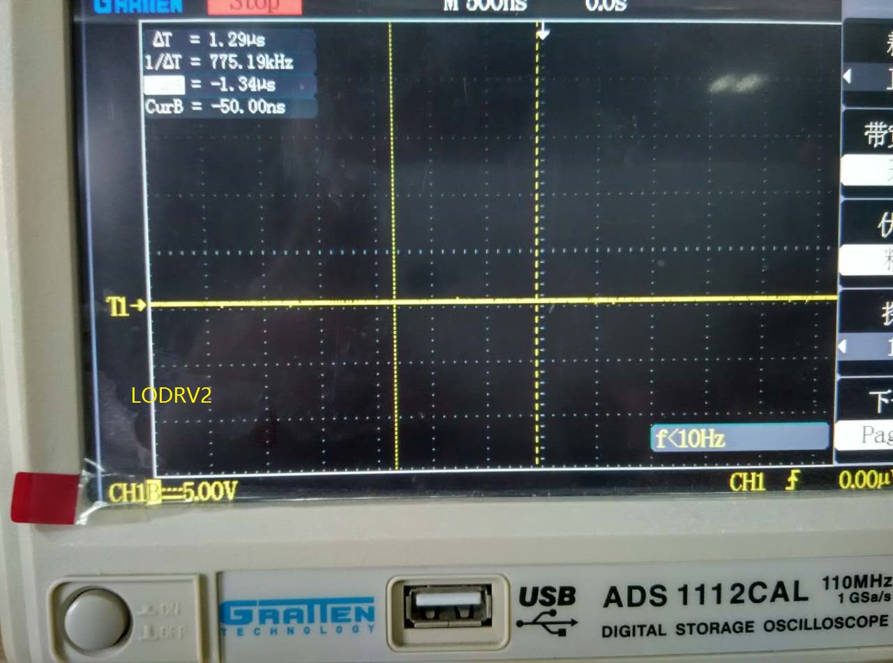
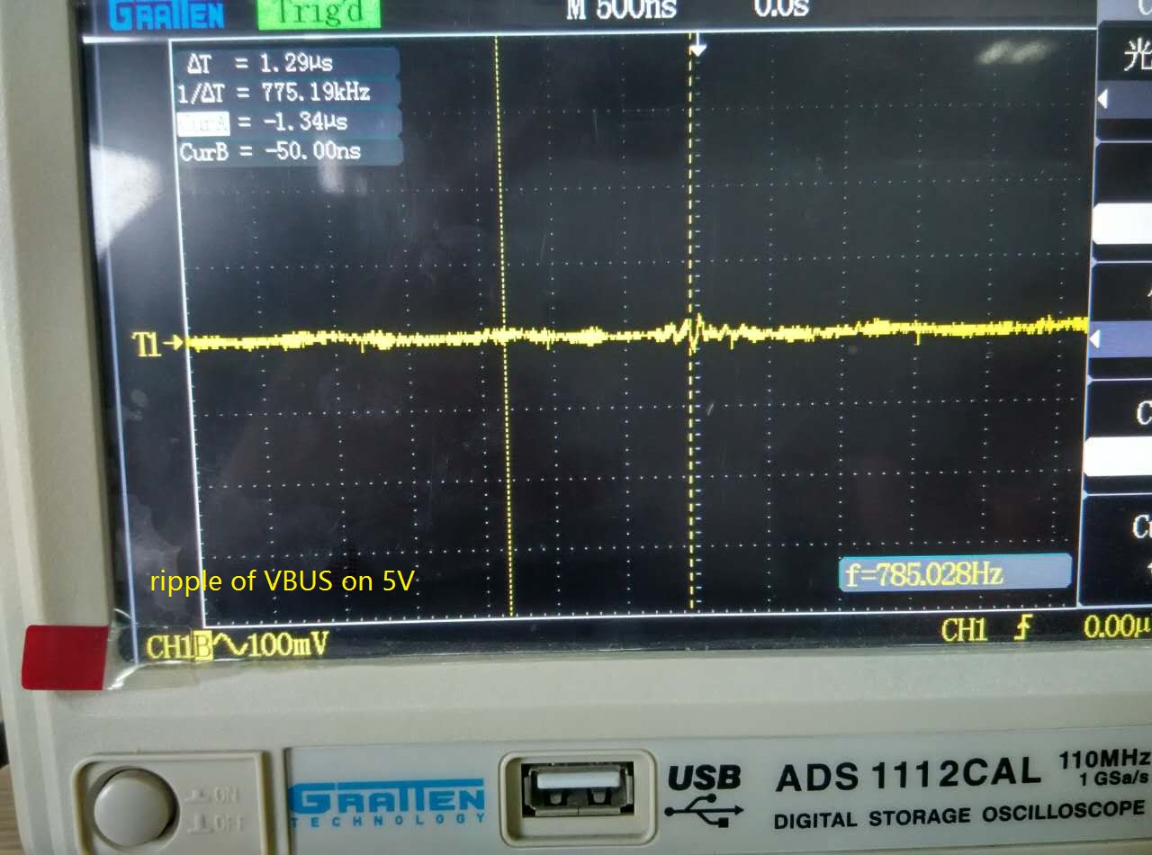
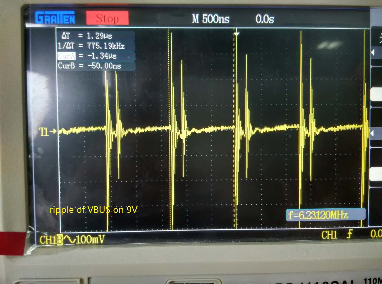
I'm now designing a power bank based on BQ25703A. When the device works under OTG mode, I found the output ripple is very large. For example, if the output voltage is 9V, the ripple is 384mV@0A, 1.39V@1A and 2.04V@2A.  Could you help me how to improve it?

Thanks

Best regards

Ren 

  • COMP2 C31 value is wrong. Please change it from 680pF to 15pF first. What is the battery voltage?

    Also, if the issue is still there, please help me zoom in the ripple. I want to see SWx, VBUS voltage on the scope picture.

  •    Dear Wang,

    Thanks.

    That's my mistake for the wrong value. I have chaged it. It is a little better but still not so good. The battery side is 7.9V. I use a power supply not a real battery.

    The VBUS side voltage can change from 5V~20V.

    Here are some more waveform. Pls help to check. The lodrv1 wave is not stable, it keep shifting, The ripple of 9V also keeps shifting slowly.

    I also changed the R34 to 10K, C33 to 33pF based on the AN: BQ25703A bom change. The issue is not removed.

    BR

    Ren

  • The waveforms are looking good to me. For 9V VBUS waveform, the probe is coupling some switching noise. You can use 20MHz bandwidth to filter the noise out. Or, measure the ripple on the input capacitor's terminal directly.

    "The ripple of 9V also keeps shifting slowly."

    1.If the switching frequency is fixed, the ripple shifting could be measurement issue. 2. Would you zoom out the VBUS ripple a little bit? So, we can see a little bit more switching cycles. Also, check the VBAT ripple. If VBAT has a big ripple, it may show up on VBUS a little bit.

  • Dear Wang,

    You are right it is related to the measurement. There are PGND and GND on my board. The VBUS is reference to PGND on BQ25703 side. And it output from a connector and change to reference to GND. The GND and PGND connect together by several vias. You can aslo check it in schematic. The ripple is 1V when I measure the VBUS and one PGND test point. It reduce to 500mV when I measure the input capcitor. It reduce to 200mV when I measure the VBUS reference to GND. And It reduce smal when I measure on load side. Do you know why?

    Thanks.

    BR 

    Ren 

  • The principle is simple. But, it may be hard to find out and prove where to make the noise because the layout is fixed.
    The ground noise voltage equals Lp*di/dt. So, we have to find where has high di/dt and which trace could have high Lp.
    On the load side, the noise could be filtered out by the load side capacitor. To me, if the load side is clean, it may be just a measurement issue because it doesn't affect the load side operation.
  • Dear Wang,

    Thanks for your great help

    BR

    Ren