This thread has been locked.

If you have a related question, please click the "Ask a related question" button in the top right corner. The newly created question will be automatically linked to this question.

BQ24600: Diode in output path

Part Number: BQ24600

Hi

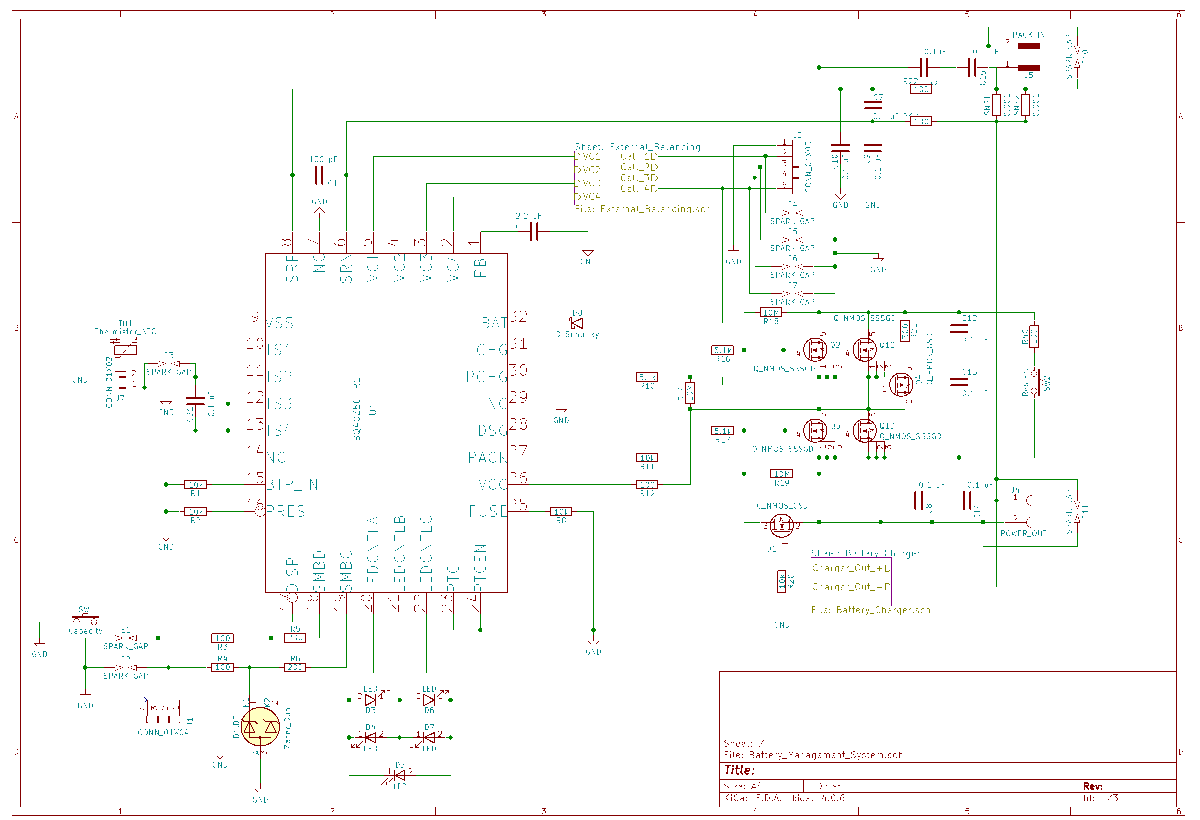
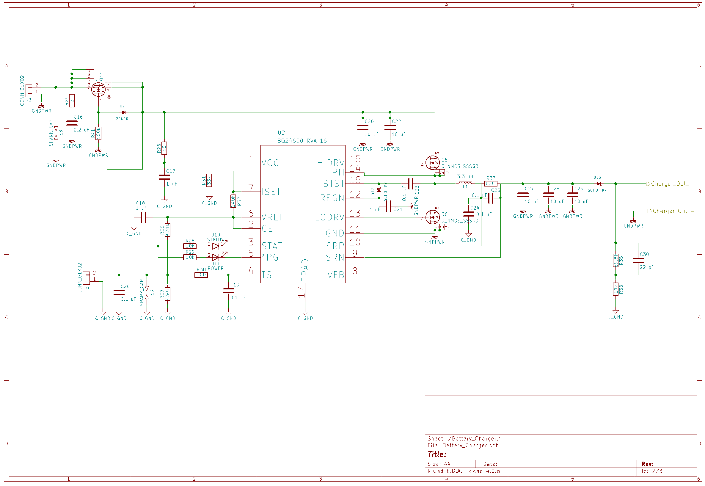
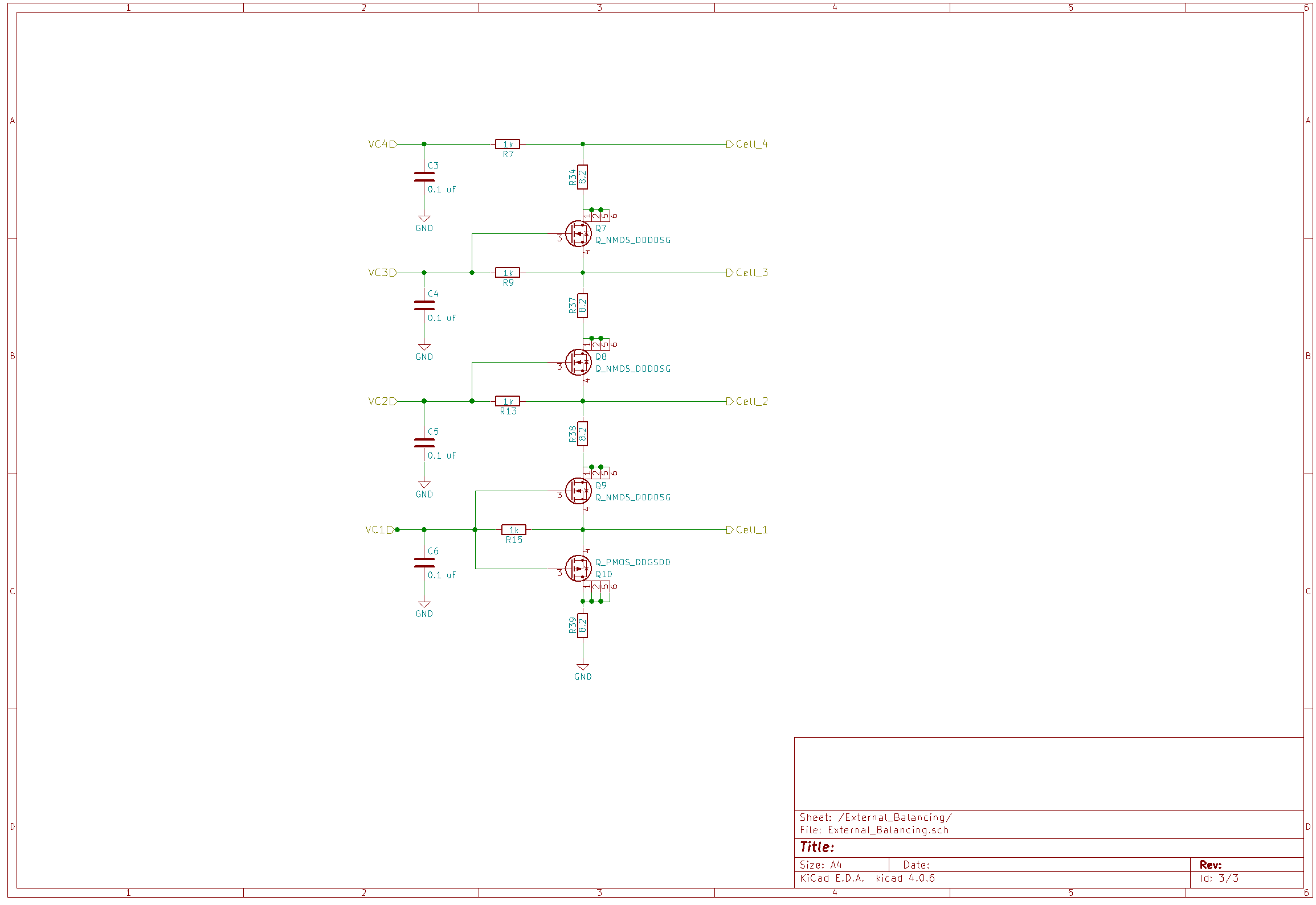
We are building a 4S (16.8V), 2A charger for a LiPo battery using the bq24600.

We had problems with the reference design as per the bq24600 datasheet: The PCB failed catastrophically from high inrush current when the battery is connected. From other post on this form it seems that several other users experienced a similar problem.

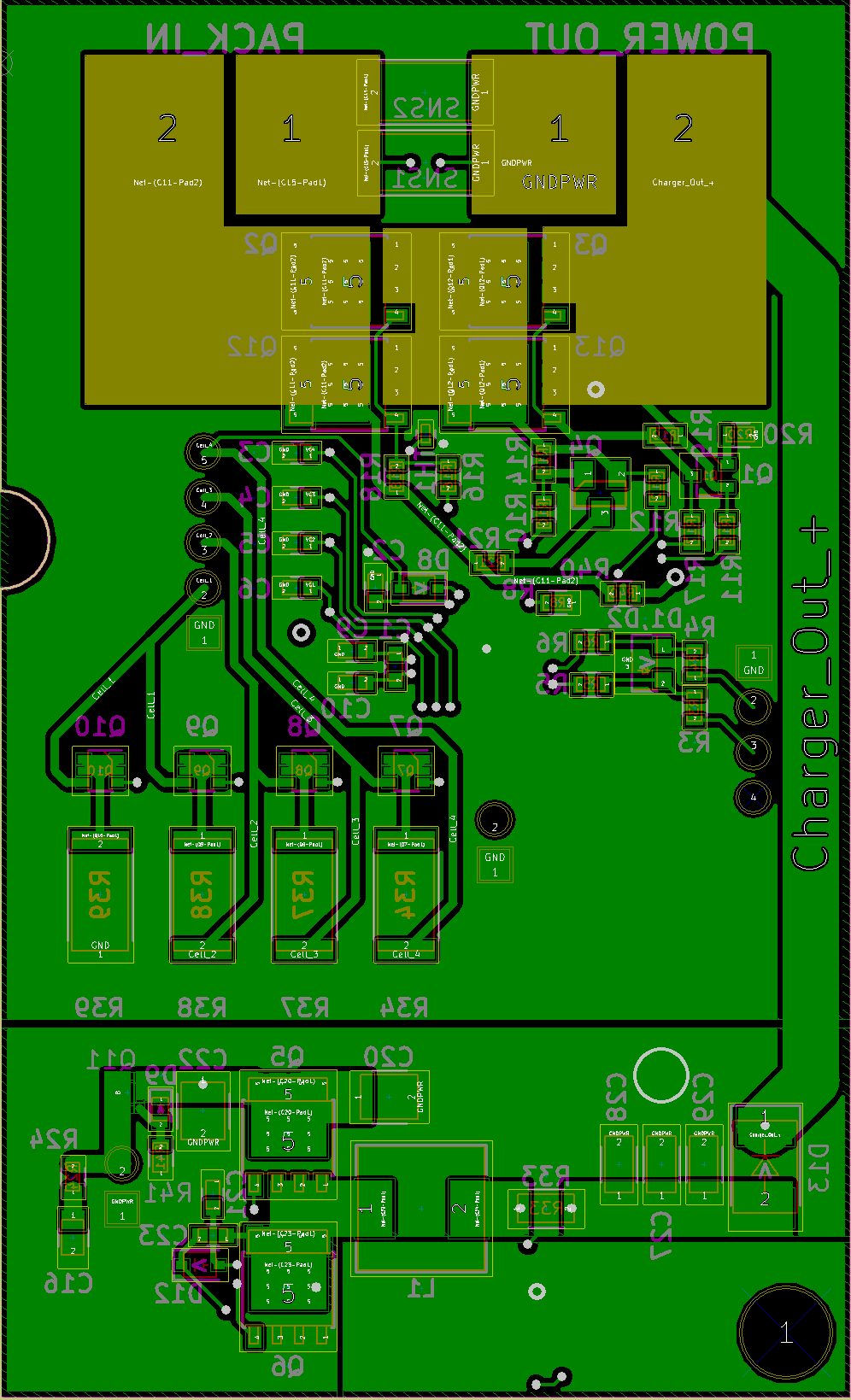
We solved the inrush current problem by simply adding a schottky diode (D13) in the output path of the charger as per the attached schematic.

However, our charge current is measured at around 1.7A and not the desired 2A as was designed for.

Thus, will the addition of the output diode affect the internal regulation of the bq24600 to explain the charge current difference? If so, what will be a possible solution for accurate charge current with inrush protection?

Thanks,

Jan-Cor

  • Hi Jan-Cor,

    Charging current depends on SRP/SRN voltage and ISET setting. Did you measure the charging current before/after adding diode? Before adding diode, is the charging current 2A or not? I need to make sure it is caused by diode or layout. Please also check the layout if it follows kelvin sensing and if GND routing is okay.

    Thanks,
    Ann Lien
  • Hi Ann Lien

    Thanks for the fast response. We did not measure the charge current without the diode because of the risk of catastrophic damage to the chip. I did manage to get one working now without the diode and the charge current is the same: 1.66A at 15.25V on the output of the charger, so the diode seems to have minimal effect.

    The voltage measured at Iset is 0.396V from a Vref output of 3.289V, so this seems good.

    It does look as if layout is contributing to the problem: we measure 17mV over the sense resistor and 18.3mV at the chip between SRP and SRN. Will look into our routing.

    Can you please elaborate on what you mean by checking that GND routing is okay.

    Any other suggestions on what else to check for charge current accuracy?

    Also, we have thermal concerns on the board as the chip temperature goes up to 90 degrees Celsius. We checked the efficiency and we have around a 90% to 92% efficiency from input to output power. However, from the datasheet it seems a 95% efficiency is what one should expect.

    What will be something to check in the layout to improve the efficiency?

    Thanks,

    Jan-Cor

  • Hi Jan-Cor,

    For the GND routing, you can check if all AGND routing(including ISET, TS, VREF) is connected to powerpad then connected to PGND. It could be the error when you didn't seperate AGND and PGND. When high current flows through analog signal sensing routing, error would be generated.

    For the efficiency concern, there are switching and conductive loss. It depends on MOSFET and driving capability. You can minimize your gate drive routing, change other FETs which has better performance.

    Thanks,
    Ann Lien
  • Hi Ann Lien

    Thanks, much appreciated. Our layout is currently optimized for small size, so our ground routing can be improved. Will revise and see if this helps with the charge current difference. Will also then incorporate better thermal considerations to try to reduce operating temperatures. Will let you know how things turn out.

    Thanks again,

    Jan-Cor

  • Hi Jan-Cor,

    Okay! Waiting for your good news!!

    Thanks,

    Ann Lien

  • Hi Ann Lien

    We revised our layout and improved our grounding. The charge current is now much better and close to the designed 2A, even with the diode.

    Unfortunately we still see operating temperatures of 85 to 90 degree Celsius for the BQ24600 chip while charging at 2A. Is there anything that you can recommend to check for potential thermal improvement or is the 90 deg operating temperature to be expected?

    Thanks and best regards,

    Jan-Cor 

  • Hi Jan-Cor,

    Is this high temperature from bq24600 or other component like MOSFET, inductor...etc.? Please help to verify which one is the hot spot so that we can discuss how to improve it. Please also provide your new layout to me for the further discussion if it is possible.

    Thanks,
    Ann Lien
  • Hi Ann Lien

    Thanks and we measured the temperatures again. When charging at 2A, the PCB board temperature is around 75 degree Celsius. The FETs are around 80 degC and the bq24600 chip is around 92 degC.

    Herewith attached is the schematics as well as the front and back board layout. Advice on what to check or change will be much appreciated.

    Thanks again,

    Jan-Cor

  • Hi Jan-Cor,

    Could you send schematic and layout(as altium file) to ann_lien@ti.com? I can check easier, thank you!

    Since bq24600 is external MOSFET solution, It shouldn't has 92 degC on IC. The only bigger power consumption is driving circuit. Could you please help me to check if driving capability is not enough for your MOSFET? or is there any big consumption in your circuit?

    Thanks,

    Ann Lien

  • Hi Ann Lien

    Our layout is being done in KiCad, an open source PCB router. I will look into the possibility of converting the KiCad format to Altium. Will be in touch via e-mail if I have more info.

    Thanks again,
    Jan-Cor
  • Hi Jan-Cor,

    Or could you please send the Kicad file first before converting? Altium is better but Kicad is also good for me.

    Thanks,
    Ann Lien
  • Hi Jan-Cor,

    It is a little difficult to check comprehensively, but I also observed some point need to verify.

    For your GND routing, GND trace of setting resistor like ISET, TS...etc. are too long. It may influence setting vallue.

    For Vin cap, you can put C20 and C22 together(at C22's position) to minimize the routing between high frequency swtiching loop.

    For REGN cap, please put it as close as possible to IC.

    For your high temperature issue, I want to check if this issue comes from IC or not. Please swap a new IC on the board to see if high temperature is still there. Also check with the impedance on old IC compared with new IC.

    Thanks,

    Ann Lien

  • Hi Ann Lien

    Thanks for the info and feedback, will look into making the proposed changes.

    Will check the IC. Can you provide more info on what you mean by checking the impedance of the IC?

    Thanks and best regards,

    Jan-Cor 

  • Hi Jan-Cor,

    Thanks for your email, I will double check the detail in your design.

    For the impedance measurement, just do a quick check to make sure old IC is still good. You can compare every pin vs. GND impedance with new/good IC.

    Thanks,

    Ann Lien