This thread has been locked.

If you have a related question, please click the "Ask a related question" button in the top right corner. The newly created question will be automatically linked to this question.

TLV62130: One of Three DC/DC downconverter often fails

Part Number: TLV62130

Support Path: /Product/Development and troubleshooting/

Hello TI-Team,

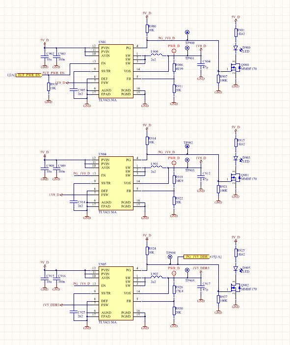
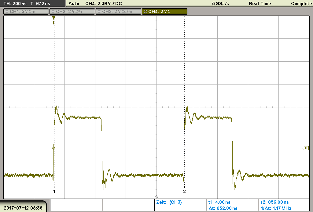
we are using 3 TLV62130 to produce the power for a xililx FPGA. The first produces the core power (1.0V) and after he ramped up,

he starts the second TLV62130, which produces 1.8V. The second TLV62130 starts the last one, which produce a 1.5V for a DDR SDRAM.

The three TLV62130 has the same layout, the only difference is the Power Enable signal.

The EN of the first TLV62130 is set by a micro controller. The micro controller has a power supply of 3.3V.

Is it possible to sent one of the defect DC/DC converter in order to get a failure report?

At which location can we sent this part?

A coppy of the shematic:

  • Hello,
    I have some questions and remarks on your schematic:
    How do you control the FSW signal? Please read the procedure in section 8.3.5. in the data sheet.
    Could you please send us the PCB layout of one converter?
    Concerning the failing device - please send it to the distributor / channel you ordered the part.
    Thanks.

    Best regards,
    Ivo

    Texas Instruments
  • Hello Ivo,

    the Layout of the U901 is send by e-mail.
    I can not copy the picture of the layout of U901 in the browser.

    Kind Regards
    Robert
  • Hello Ivo,

    I can not send an e-mail, because it is non reply.

    Now I found the solution.

    Thank you.

    Kind Regards

    Robert

  • Hello Robert,

    thanks a lot for sharing the layout.
    The power net routing really looks excellent !
    However one important item is the sensitive VOS pin connection.
    So could you please also share the inner layer trace from FB resistor (R906) to VOUT capacitor (C904) and VOS pin of the device?

    Best regards,
    Ivo
  • Hello Ivo,

    thank you for your response. The Layout with the internal connection:

    As described in your datasheet, we connected the FSW pin to Vout:

    Your Specification for low is 0.3V and for high is 0.9V, that means we are above the high level (1.0V).

    What happend if we would be under 0.9V. We measured the output level of 1.0V and we are stable.

    Our EMS had bought the device at Digikey. They will deliver the defect device. The EMS has to fill out the documents. 

    How can we synchronise our corresponding correspondence with the failure report?

    Kind Regards

    Robert

  • Hello Robert,

    thanks for sharing the complete layout. It looks good, there are no concerns.
    I also noticed that FSW is connected to VOUT. With a VOUT setting of 1.0V, the high level will be well detected.
    Don't worry, we will be able to synchronize the failure device if you mention the headline of the e2e correspondence in the document.
    By chance do you have some more information about the failing mechanism - e.g. fails at power-up or during run time? Or do you have any indications about the defect (e.g. input or output shorted)?
    Thanks.
    Regards,
    Ivo
  • Hello Ivo,

    I have mentioned the headline.

    We have a startup sequence when we power all our boards, but we haven't a power down sequence yet. We have a uC, which do this. We have also 2 arm processors, which have to store the state before they power down. This is still not implemented by software, so we turn down the AC/DC power supply. After we turn it on, the U901 doesn't start. It also failed, when the power supply is a laboratory power supply.
    After we had 6 failure, we decided to sent you one DC/DC converter for analysis, to get know which part of the IC is defect.
    May be we get an idea, whats going wrong.

    Kind Regards
    Robert
  • Hello Ivo,

    we measured the SW Pin of DC/DC converter 1.0V and 1.8V. The switching frequence should be 1.25MHz: in fact it is 1MHz (80%) an there is a step before he switches to the top transistor.

    The 1.8V looks better: There is no step before he switches on the top transistor, but his frequency is 1.17MHz (93.6%)

    Kind Regards

    Robert

  • Hello Robert,

    thank you for the scope plots of the SW node wave form. This looks ok: With VIN < 6V the switching frequency can be lower than the typical 1.25MHz. Also the short negative step is a normal behavior.

    You mentioned that currently a lab power supply is used to power up and down the PCB.

    Hot plugging can create high voltage transients damaging the device.  Please read this blog explaining the phenomenon and workaround by adding a larger tantalum capacitor at the input:   https://e2e.ti.com/support/power_management/non-isolated_dcdc/f/196/p/608918/2243806#2243806 .

    Best regards,
    Ivo

  • Hello Ivo,

    thanks for your e-mail.

    There is a problem with the link of the block: I think the link is false, because I get only my post.

    Kind Regards

    Robert