Hello,
I'd like to implement tracking and AVS functions with TI's TPS54020RUWR regulator. (PON chip requirement.)
Can you share common applications of schematics?
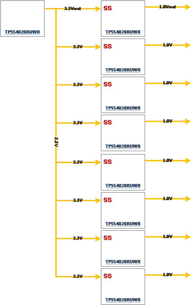
Eight TPS54020RUWRs should be supplied to each of the eight chips in total, with 1.0V, and the following functions should be included.
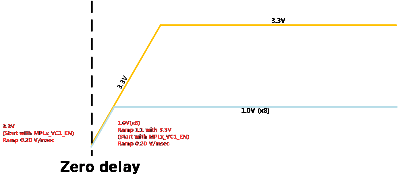
1) 3.3V tracking (3.3V output from other regulator should be 1.0V power-up at the same time, 0.1V-> 0.2V-> 0.3V at the same time.
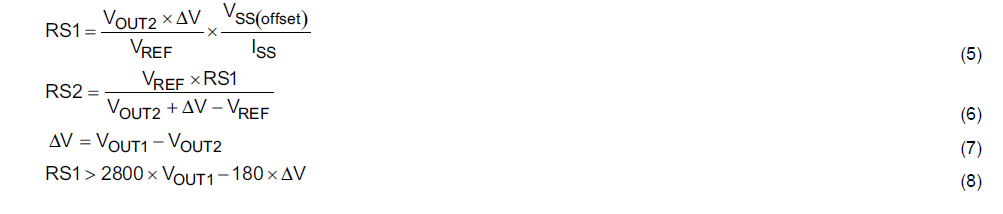
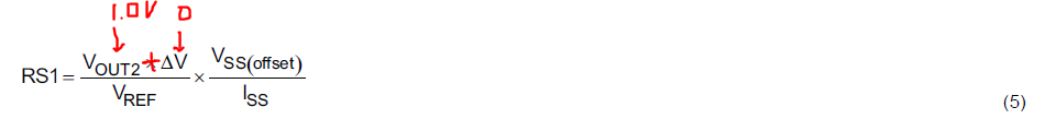
The datasheet 16 page describes how to implement the related functions. I do not know if it is accurate. Please confirm.)
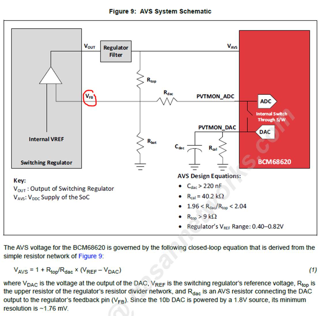
2) AVS function (connect PVTMON_ADC of PON chip to feedback pin of regulator. I do not know which pin is used for feedback function.
Please confirm.)
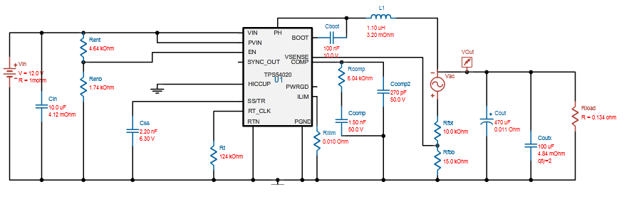
TPS54020RUWR
Each input voltage: 12V
Each output voltage / Max current: 1.0V / 7.476A
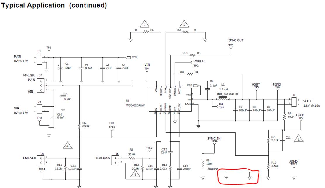
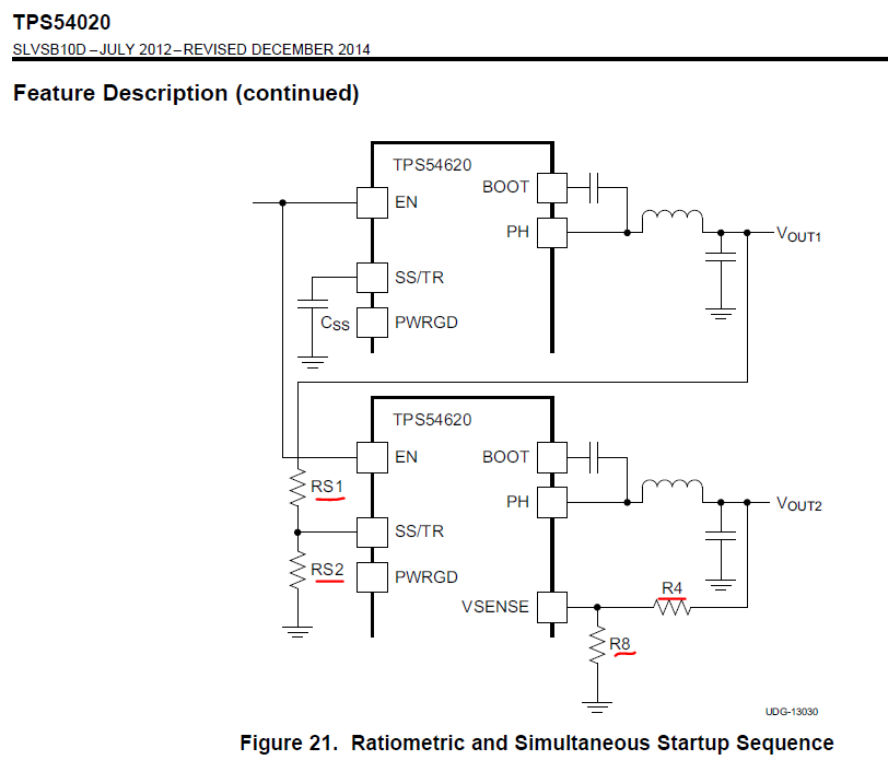
3.3V tracking
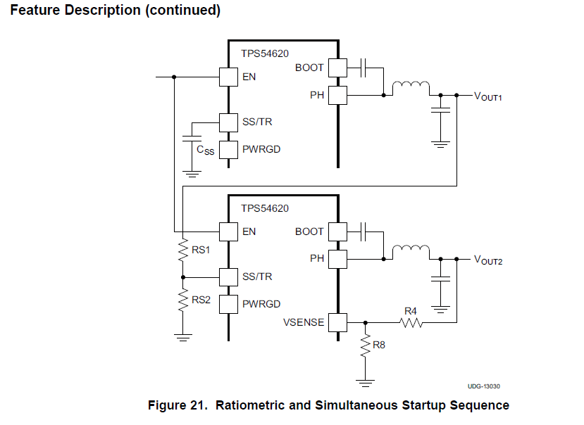
HW structure between PON chip <-> regulator for AVS implementation is as follows.

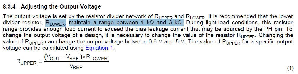
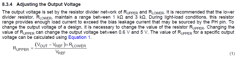
I have a question. In the datasheet, what exactly are the resistances of R upper and R lower?
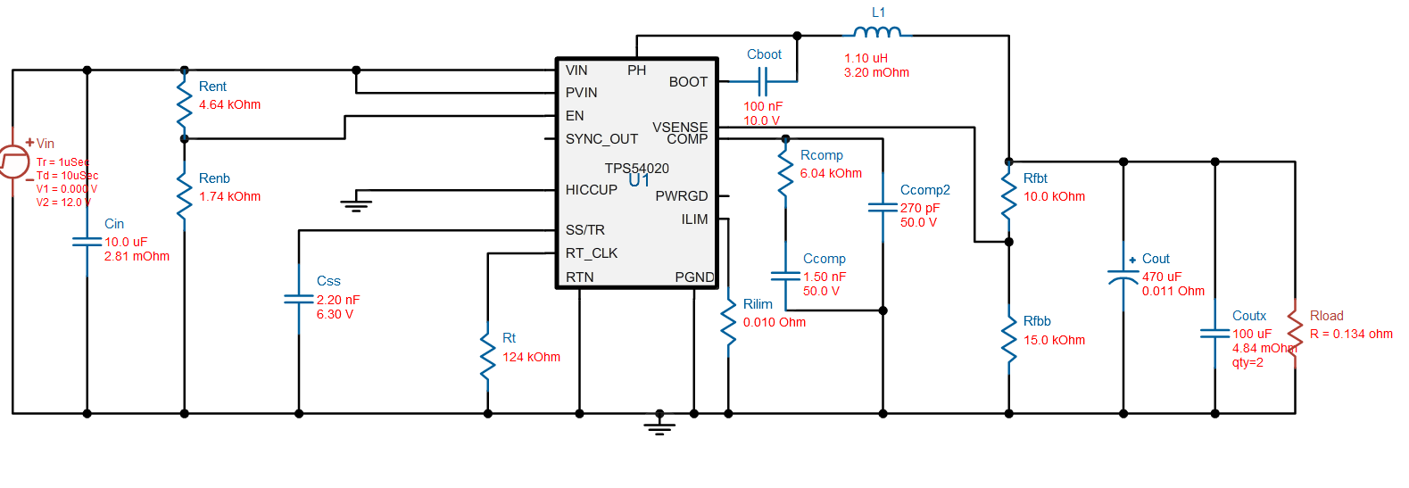
The TI simulation results are shown below.
The power structure is as follows.

thanks,
TS