This thread has been locked.

If you have a related question, please click the "Ask a related question" button in the top right corner. The newly created question will be automatically linked to this question.

LM25069: IC not giving output on connection of a capacitor load.

Part Number: LM25069
Other Parts Discussed in Thread: CSD18502KCS

Hello,

The project I am working on involves using the LM25069-2 as a load protection circuit of a microcontroller. The circuit has been designed according to the recommended circuit in the datasheet. The evaluation module of the microcontroller has a total capacitance of 245 uF. When no load is connected to the output, LM25069 gives an output of 3.3V (which is the input). But on connecting the evaluation module, the output voltage drops close to zero. 

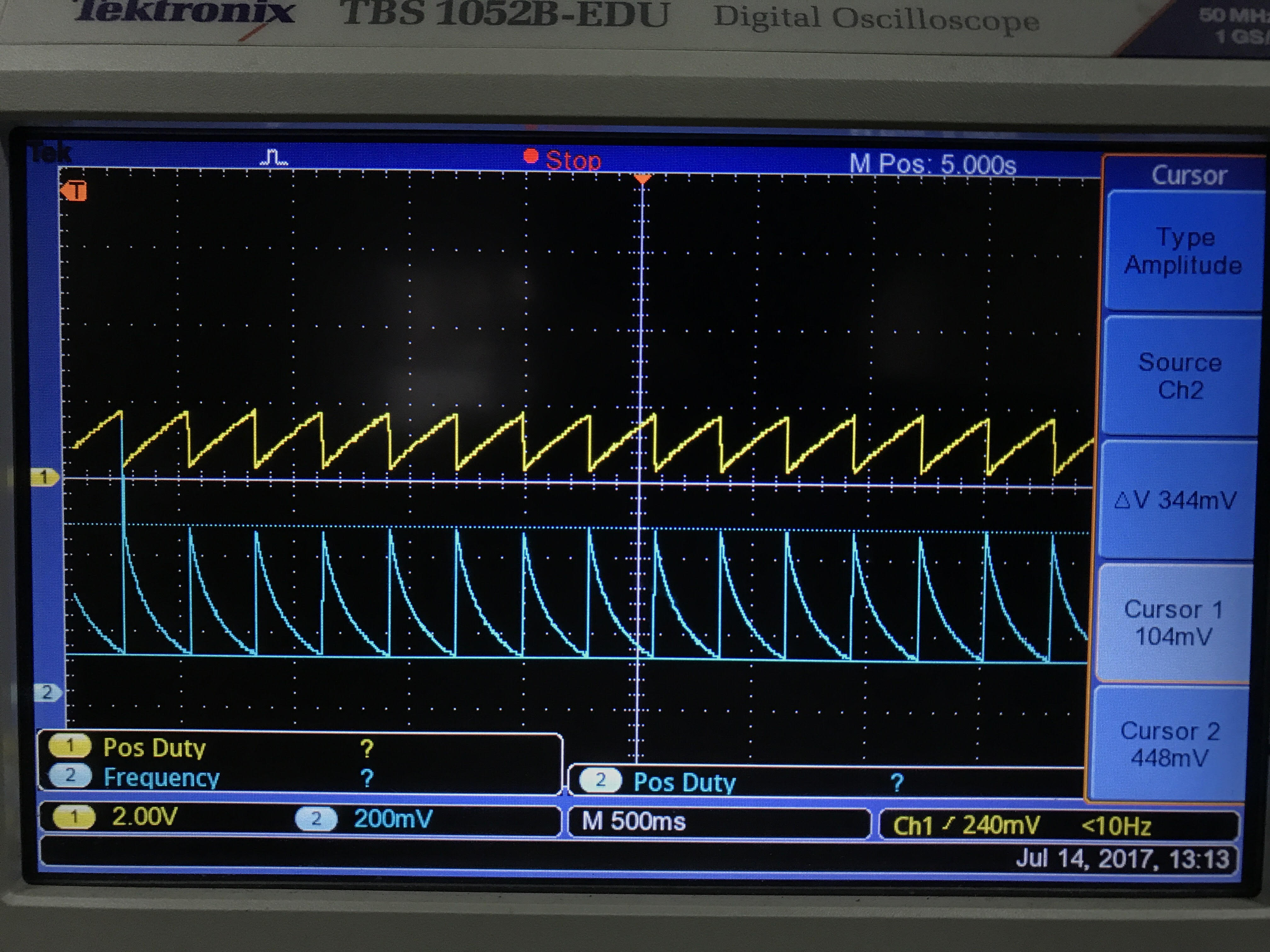
Yellow: Timing Capacitor(The rise time is 280 ms)  Blue: Output (Ripple between 104 mV and 448mV). The gate pin gives a high signal during the fall time of the yellow wave (which is actually just a spike of 1.5-2V) and during the rise time it is low.

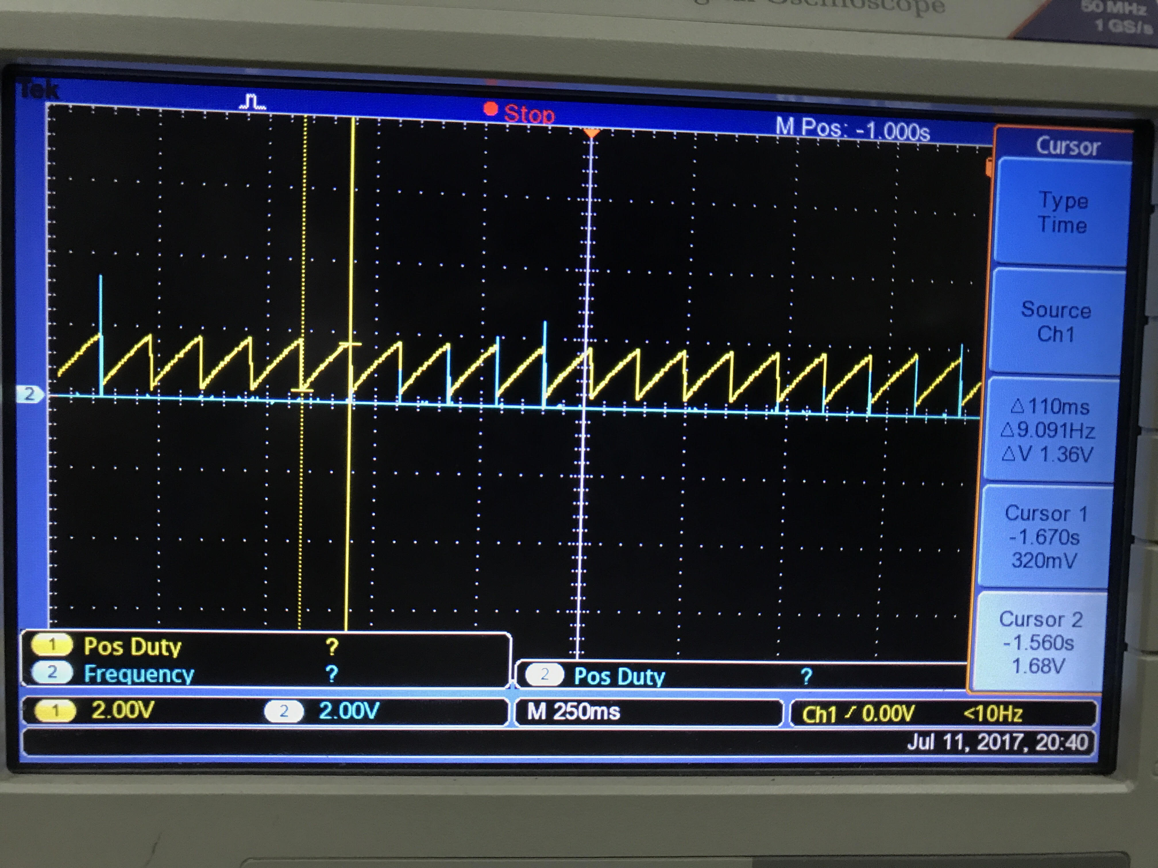
The yellow wave form goes from 0.3V to 1.72V and has a time exactly of insertion delay.

The waveform suggests a net resistance parallel to the load capacitors of about 1.8 kohm.  Based on this the turn-on time was calculated to be 0.8 ms . insertion delay is 278ms. Timer pin has a capacitor of 0.89uF. Fault timeout is set at 15.8ms. 

A current limit of 1A was set initially but later when the sense resistor was shorted no change was observed in the output. UVLO and OVLO are set at 2.9 and 3.5V respectively and hysteresis of both is close to 0.1V.  No resistor is connected at Rpwr as that function was not needed.

I went through all the parameters in the datasheet but still can't figure out why the output is unable to rise to its normal 3.3V but couldn't find anything. Has anyone seen something similar happen? What can I do to resolve this?

  • Ajinkya

    The circuit may be in CL / CB Tripped or possibly PL from the scope shot.  Look at the rising output dv/dt and calculate the current into the output capacitance.  Use a current probe and measure the input current along with Vin_Vout_Vgate so you can see gate action and also determine the FET power throughout the timer period.  What does Vin look like the whole time?  Is it solid or is there an input voltage issue?  Is there a load on the output other than the output capacitance when power up? Assure that the current sensing is kelvin sensed (see DS figure 27) and that the Vin route to the IC is short and thick etch as this serves as both current sense and Vbias.  Any voltage on this route can impact CL point.  It's ok to power up into CL as long as it is set to allow for Cout to fully charge before the timer trips and you are not violating the FET SOA ( i don't think you have a bown FET here).  Make sure the Vin capacitor is located at the Shunt "+" side, not at the Vin pin of the IC.  This provides both CM and DM filtering for current sense, better than if at the IC.  You can also inserte a 2 ohm resistor in the "sense" line and a .22uF capacitor from "Vin" to "Sense" for filtering (don't put the 2 ohm in the Vin line due to bias current into that pin).

    You can try to adjust the Rpwr to check for PL.  Raise its value to see impact.  Recommend above current probe measurements before you try this.

    If you need to adjust dv/dt due to higher than anicipated Cout, then  use the attached BJT circuit.

    BrianBJT Circuit.pdf

  • Hi,

    The sense resistor was shorted and still the issue persisted. So, the circuit is not in current limit or circuit breaker fault. The power limit pin has been left open and thus the circuit can’t be in power limiting either.

    The input voltage is a constant DC without any glitches.

    As mentioned in the earlier post, the fault timeout has been set considering the time taken for the capacitor to charge.

    The Mosfet used is csd18502kcs

    The microcontroller is the only load on the IC during power up, but as mentioned in the earlier mail, it seems, from the output voltage waveform, that the load can be modelled as a capacitor and resistor in parallel (245uF and 1.8k ohm).

    In the image the blue waveform (overlapped on yellow waveform) is voltage at the gate pin and the yellow is the voltage at the timing capacitor.

    It appears (form the snapshot posted in the first post) that the capacitor at the output gets charged upto 448mV when the gate is going high (a spike during the falling edge of the timing capacitor waveform as seen in the image) and during the time when it is low, the capacitor is discharging through the modeled resistor parallel to it. I tried reducing the rise time of the pulse and changing the current limit so as the net result of the charge-discharge cycle will be positive, but that too didn’t help. 

    I will try implementing the BJT circuit.

    Is there a doc that I can refer for the same?