This thread has been locked.

If you have a related question, please click the "Ask a related question" button in the top right corner. The newly created question will be automatically linked to this question.

BQ76920: In BQ76920 there is a Pulsating signal at CHG MOSFET and output of the Battery Pack is not Stable.

Part Number: BQ76920


Hi

I am using BQ76920 for BMS and controlling it through ATtiny 24A for which I have set the Registers as following

SYS_CTRL1 , 0x10

SYS_CTRL2, 0x43

PROTECT1, 0x9F

PROTECT2, 0x1F

PROTECT3, 0x00

Sense Resistor which I am using is 33 mOhms as for MAX Short Circuit Current to be 5 Amp and Max Charging Current to be 2.5 Amp

My observed Waveform is as Follows (where RED Waveform is of Gate of (CHG) N-MOS)

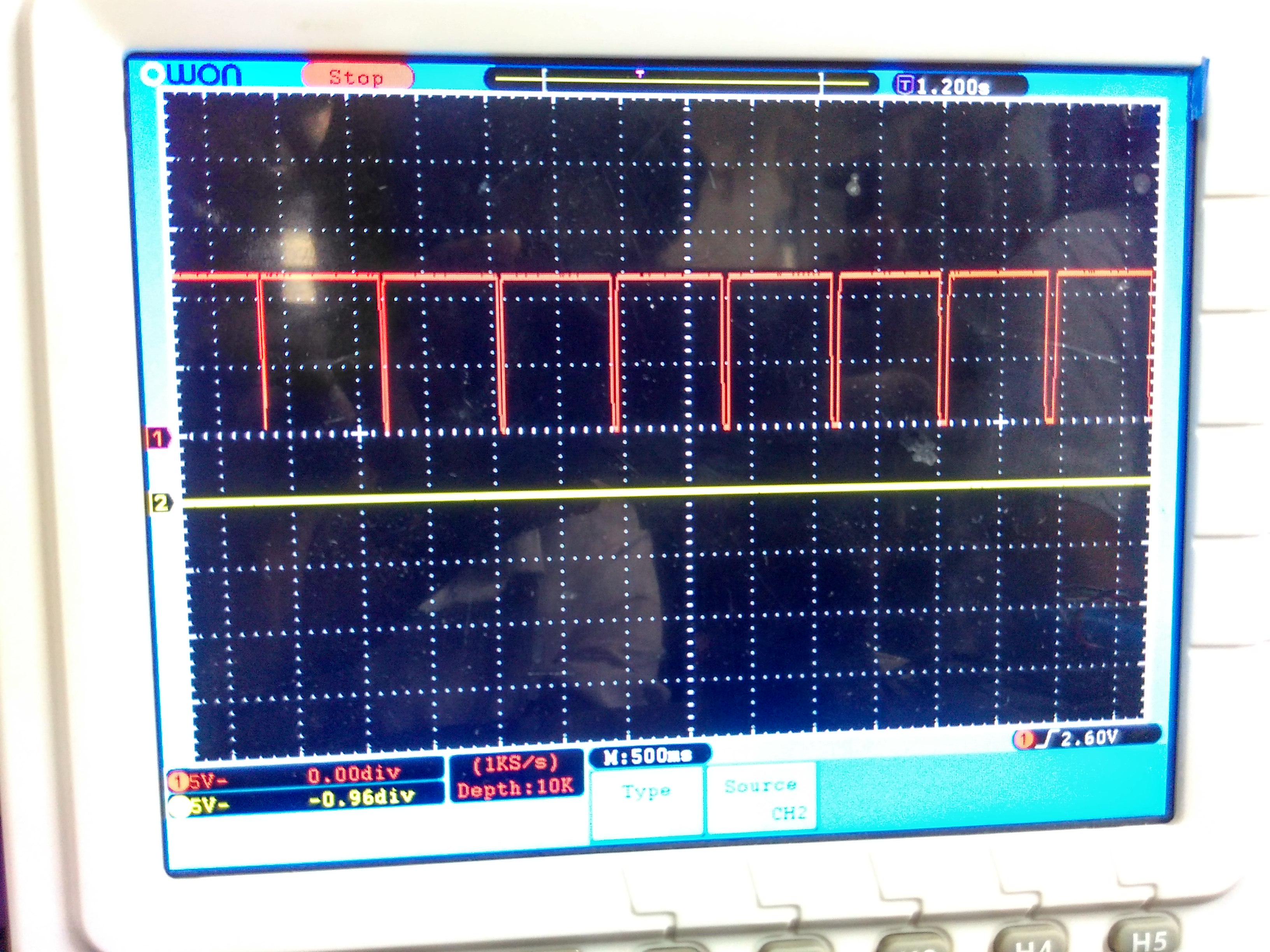
I would like to know, whether on Monitoring the Battery, the Main Supply is been disconnected to Read the Exact Battery Voltage or while CC Reading ??? Whether it is a Issue with the Peripherals OR or Register Setting ??? 

  • I would Also Add here that I am clearing the SYS_STAT and Enabling the CHG and DSG bit of SYS_CTRL2 in an infinite Loop after checking the status and Clearing the fault. with a time interval of 250ms.
  • Dear designer,

    Seems the ALERT is spuriously false triggering due to lack of noise immunity.

    Need Time constant on pulldown to settle within ~ 250uS to avoid the part from detecting residual ALERT pin voltage after status register CLEAR. For noise immunity , use time constant= 250uS. Suggest using [R=500K,C= 500pF] filter to GND.

    hope this helps you out.

    thanks

  • Hi vish

    Thanks for the advice

    I would like to add a very interesting point here that I am already using the pull down of similar configuration to provide time constant of 250uf. And as what have I observed?  At the alert pin there is no High signal at the time when MOS is getting off.  Also as we can clearly see here above that the state change is taking place every 800ms approx.  And which is off for nearly max upto 120ms approx.  Then is set manually on by the host as what I am doing in an infinite loop in the code at an periodic interval of 250ms

    I did also found that gate drive of CHG MOS showing the above mentioned behavior when ADC bit of SYS_CTRL1 is enabled. As when I disabled the ADC,  it indeed mat have disabled the OV and UV protection till next transition from ship mode to Normal Mode.

    I didn't understood this behavior???

  • State Change? Are you referring to SHIP to NORMAL mode? Per d/s pp21. it takes about 800ms before reading out initial cell voltage data.
    For MOS tun-on/off/on behavior,suggestion would be to decrease the G/S pull-down resistor. decrease the value, will have stronger pulldown of the FET. i/e, If using 1M, then try 400K for both.