This thread has been locked.

If you have a related question, please click the "Ask a related question" button in the top right corner. The newly created question will be automatically linked to this question.

WEBENCH® Tools/TPS54360-Q1: High frequency for small inductor size compromising efficiency

Part Number: TPS54360-Q1
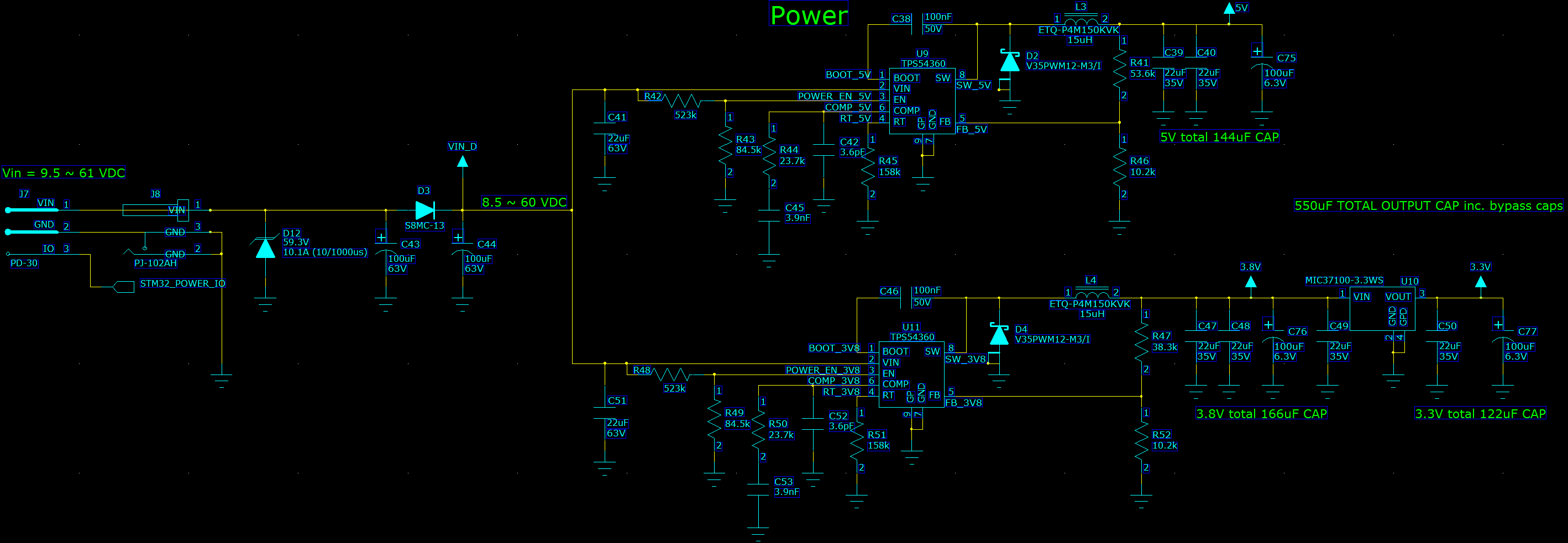
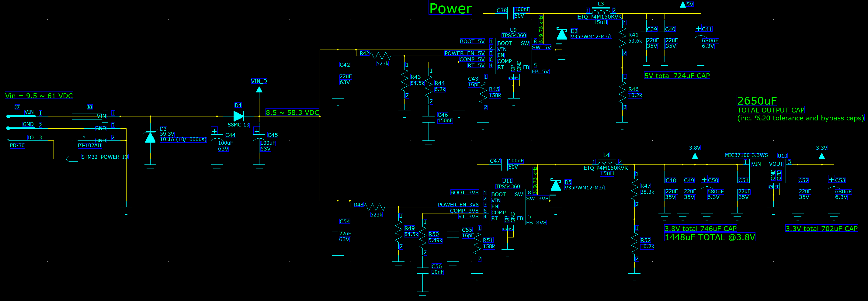
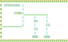
Other Parts Discussed in Thread: TPS54360, TINA-TI

Tool/software: WEBENCH® Design Tools

Hi,

I would like to design a circuit as small as possible by increasing the frequency. However, when I increase the frequrncy using WEBENCH tool, the automotive grade TPS54360-Q1 disappears from the list. and nothing shows up at 1500KHz although they can go up to 2500KHz.

Anyone have any idea what is going on here? How can I test the circuit with such purpose?

Any helps or comments are appriciated.

Regards,

Ogulcan

  • Can you post your webench inputs? We can try to duplicate it.
  • Vin : 6V ~ 60V
    Vout : 5V
    Iout : 3.5A

    My switching frequency target is 2000 KHz, and I'm trying to put the smallest inductor possible.
  • I also want to use 2 buck converter chips which are both TPS54360-Q1. If there are components that can be shared, I would like to hear that too. For example maybe I can use the same circuitry of RT, SS and COMP pins.
  • Webench thinks the maximum switching frequency for your design is 617 kHz. It is limited by fskip max of Eq eq 9 in the datasheet. You can possibly share some component values between your two designs. If you use the same frequency, then RT is the same. If you use the same slow start time then Css is the same, etc.
  • This makes no sense as the datasheet clearly indicates that the maximum switching frequency is 2500 KHz.

    Although the WEBENCH limits the fs like this, there has to be a workaround I guess? Otherwise, TI has to change the fs range of this component.
  • There are several variables that work into the fsw max skip and fsw max shift equations. Not every possible design can work at the maximum frequency. In your case, the required on time will be less than the minimum controllable on time at switching frequencies above 617 kHz. If you set your switching frequency higher your circuit will skip pulses.
  • Okay, this option is unacceptable in my case. What if I use TPS54360, the one which is not automotive grade. Although we will use it inside a truck, it is not required to be automotive grade. Any other swithing regulator option is welcomed.
  • All the parts in that family have the same function with regard to the switching frequency. Can you lower your maximum VIN? That is what is causing the Fsw limitation.
  • Hi,

    I cannot lower my VIN max value as the input voltage may reach such values in the truck environment, however I can use larger inductors if I can share some components. Because I will use two buck converter IC, one for 5V, other for 3.8V.

    So, is it possible to share EN, COMP and RT pins in a case where we use the same buck IC, i.e. TPS54360?

    Thanks,
    Ogulcan
  • I think what you are asking is not "Can I use the same component values for the two converters?" but actually "Can I use the same physical components such as one RT resistor connected to both ICs?". If it is the first case, the answer in most likely yes. If it is the second case, you can possibly share SS capacitor and maybe EN resistors, definitely not COMP components. I would not recommend sharing RT resistor either as RT/CLK is noise sensitive. In any case, these should be small components physically (you can use 0402 or even 0201 if you want to save space).
  • Hi John,

    Thank you very much for such valuable information. You are right, I meant physically the same components.

    I've decided to use 0603 to be the smallest package throughout the overall design and there are cases where you cannot find smaller packages such as 47uF which is 1210 for 6.3V endurance voltage.

    At this point, I would like to ask if I can use any approach to lower these output capacitor values.

    Does putting TVS diode at output helps to lower output capacitors? I also would like to build a failsafe design so I was considering TVS option anyway, thus I would like to hear your opinion about putting TVS at output for a failsafe design.

    Ogulcan

  • Output capacitance value is mostly dependent on your transient response needs. During a sudden load step increase, the additional current is supplied from teh output capacitor and will cause the output voltage to drop and on a sudden decrease in load current the excess current goes into the output capacitor causing the voltage to rise. The amount of droop and rise decreases with increased capacitance. So if you do not have load changes, you may reduce capacitance. Whether or not you use a TVS does not matter in this regard.
  • Okay, I may consider to put electrolytic capacitors here if I have the chance to put it away from the IC or the inductor like 20mm distance.

    Another problem I am facing is the inductor selection. Here I check the test frequencies of the inductors (in addition to inductance and saturation current). Thus, what can be the test frequency of the inductor if I intent to use 604 KHz as the switching frequency?

    What do you think about the effect of the TVS diode at the output for a more failsafe design?

    Ogulcan

  • For inductor selection, you can use one of the selection tools here:

    http://www.coilcraft.com/

    The TVS can limit over voltage faults if you need that.
  • i think this is answered.  Let me know if you have further questions.

  • Well.. I'm planning to post my circuit for a review and maybe someone also get inspired form it.
  • Hi John,

    Do you have any comments about the schematic?

    Regards,
    Ogulcan
  • Did you have a specific concern? How did you calculate the component values?
  • Hi John,

    I've used WEBENCH tool to simulate the values, used it directly.

    But I'm planning to put extra 3000uF output capacitance all around the PCB (150mmx100mm area) in order to make it more durable to short electric cuts. If I can find space, I may put some extra capacitance (few hundreds) at the input as well.

    My only specific concern is its being failsafe and handle harsh automotive current spikes and/or voltage instabilities. Apart form that, I just need a general overview, that's all.

    Regards,
    Ogulcan

  • Hi,

    Here is my latest schematic for review.

    What do you think about the output capacitance?

    Regards,

    Ogulcan

  • Mixing dielectrics with your output capacitors can make compensation more challenging. I suggest you ceck the loop response using the pspice average model available here:
    www.ti.com/.../toolssoftware
  • Hi John,

    Thanks for your feedback, I've been working on the compensations for a while.

    I managed to put larger capacitors to the output, so I made the calculations according to the above circuit;

    I had some difficulty in building the circuit in TINA-TI, however I managed to do the calculations using Octave (octave.org). Copying and pasting the above code will do the work;

    Ioutmax = 3.5; # maximum output current
    Vout1 = 5; # 5V output
    Vout2 = 3.8; # 3.8V output
    RESR = 40e-3; # ESR at output (roughly same)
    Cout1 = 724e-6; # output capacitance of 5V
    Cout2 = 1448e-6; # output capacitance of 3.8V
    gmps = 12; # power stage analog transconductance = 12A/V
    gmea = 350e-6; # error amplifier transconductance = 350uA/V
    Vref = 0.8; # reference voltage
    fSW = 619.76e3;# switching frequency
    
    RESRref = 2.5e-3; 
    Coutref = 58.3e-6;
    
    ################################################################################
    # REF #### REF #### REF #### REF #### REF #### REF #### REF #### REF #### REF ##
    ################################################################################
    # Reference design calculations for clarity
    fPref = Ioutmax / (2*pi*Vout1*Coutref) # 1911 Hz
    fZref = 1/(2*pi*RESRref*Coutref) # 1092 kHz
    fcoref1= sqrt(fPref*fZref) # 45.68 kHz
    fcoref2= sqrt(fPref*600000/2) # 23.93 kHz
    fcoref = min(fcoref1,fcoref2)
    Rref = (2*pi*fcoref*Coutref/gmps)*(Vout1/(Vref*gmea)) # 13 k --goal 13k
    C1_ref = 1/(2*pi*Rref*fPref) # 6.38 nF --goal 6.4nF
    C2_ref = Coutref*RESRref/Rref # 11.17 pF --goal 11.2pF
    ################################################################################
    ################################################################################
    
    ################################################################################
    # 5V #### 5V #### 5V #### 5V #### 5V #### 5V #### 5V #### 5V #### 5V #### 5V ##
    ################################################################################
    # calculating fP1, fZ1, fco1 for 5V switching regulator
    fP1 = Ioutmax / (2*pi*Vout1*Cout1);
    fZ1 = 1/(2*pi*RESR*Cout1);
    fco1_1 = sqrt(fP1*fZ1)
    fco1_2 = sqrt(fP1*fSW/2)
    fco1 = min(fco1_1,fco1_2)
    # 5V resulting values
    R1 = (2*pi*fco1*Cout1/gmps)*(Vout1/(Vref*gmea)) # 6.2251 k (6.2k)
    C1_1 = 1/(2*pi*R1*fP1) # 166.15 nF (150nF)
    C2_1 = Cout1*RESR/R1 # 4.652 nF (4.7nF)
    ################################################################################
    ################################################################################
    
    ################################################################################
    # 3V8 ### 3V8 ### 3V8 ### 3V8 ### 3V8 ### 3V8 ### 3V8 ### 3V8 ### 3V8 ### 3V8 ##
    ################################################################################
    # calculating fP2, fZ2, fco2 for 3.8V switching regulator
    fP2 = Ioutmax / (2*pi*Vout2*Cout2);
    fZ2 = 1/(2*pi*RESR*Cout2);
    fco2_1 = sqrt(fP2*fZ2)
    fco2_2 = sqrt(fP2*fSW/2)
    fco2 = min(fco2_1,fco2_2)
    # 3.8V resulting values
    R2 = (2*pi*fco2*Cout2/gmps)*(Vout2/(Vref*gmea)) # 5.427 k (5.49k)
    C1_2 = 1/(2*pi*R2*fP2) # 289.69 nF (220nF)
    C2_2 = Cout2*RESR/R2 # 10.67 nF (10nF)
    ################################################################################
    ################################################################################

    So, what I'm not sure about this compensation loop values is whether I put the nearest values or the smaller (or larger) values. This depends on whether the values are calculated specifically or could be under or below a limiting point.

    What I mean is, for example; I set the first resistance to be 6.2k. Do this value determine the lower limit so that it can also be 5k, or it has to be specifically 6.2k?

    Thank you.

    Regards,
    Ogulcan

  • I don't think that algorithm will work with mixed capacitor types in the output. You will not have a single ESR zero, but a zero / pole / zero instead. I would use the regular TPS54360 pspice or TINA-TI average model to check the compensation.
  • I think this thread is resolved off line...
  • Hi John,

    Sorry for such a long thread.

    I will continue my simulations in mostly TINA-TI and hopefully finish today.

    In the meantime, here are my PCB drawings in 2D and 3D:

    Note that some capacitor 3D models are wrong, so no worries about that issue.

    Regards,

    Ogulcan