Part Number: TPS65130
Hi,
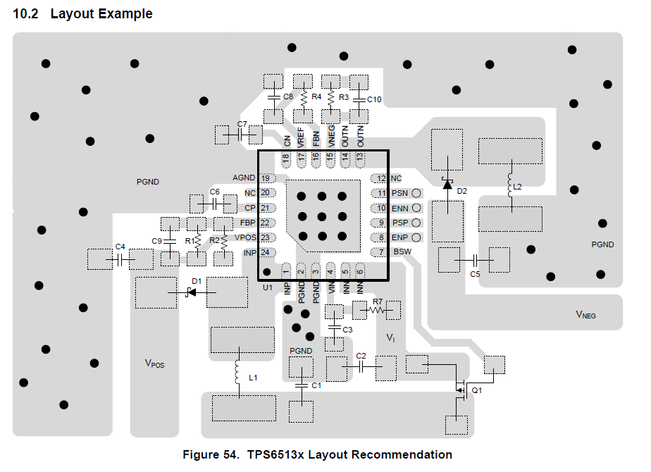
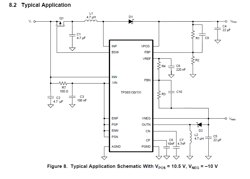
I'm trying to layout a board containing the TPS65130, so I'm following the layout example given in the datasheet (copied below). However, I have a few questions. In the example schematic given (also shown below), R3 and R4 both connect to FBN (pin 16); however, in the layout example, there is no trace drawn to R3. Why is this? Was that just an oversight, or is there a reason they would not be connected?
Additionally, I was wondering why pins 8-11 don't seem to connect to anything in the layout example. Can they be left floating, or are they just left like that to show that it is up to the user where to connect them (ie, they can either be connected to high, ground or some digital logic pin, etc.)?
Thank you for your help!
Matt