This thread has been locked.

If you have a related question, please click the "Ask a related question" button in the top right corner. The newly created question will be automatically linked to this question.

TPS54020: question about Ratiometric and Simultaneous Startup Sequence

Part Number: TPS54020
Other Parts Discussed in Thread: TPS54623,

Hello TI,

I have already asked a question in the following article, but it has become too long and I am rewriting it.

https://e2e.ti.com/support/power_management/non-isolated_dcdc/f/196/p/609676/2270102#2270102

In sum, yy question is below two now.

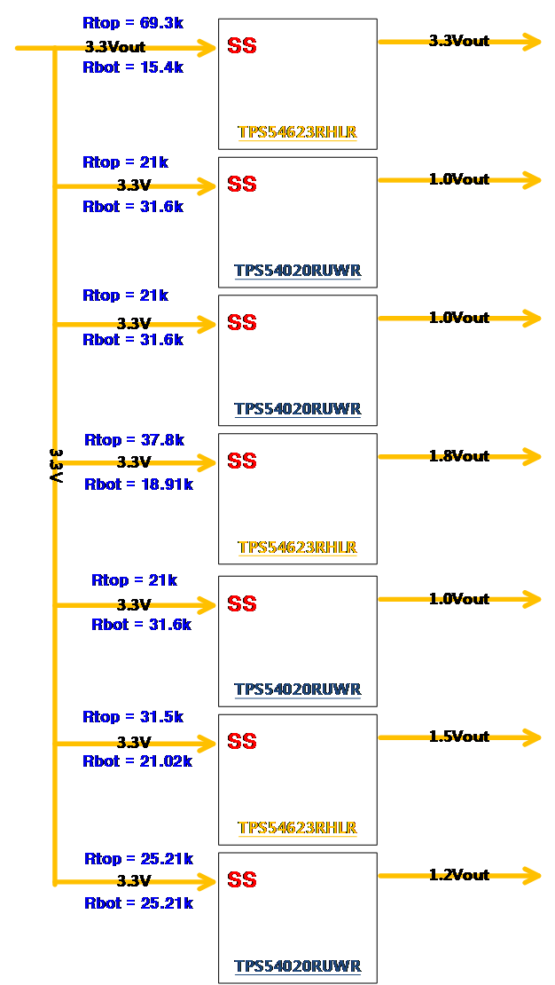
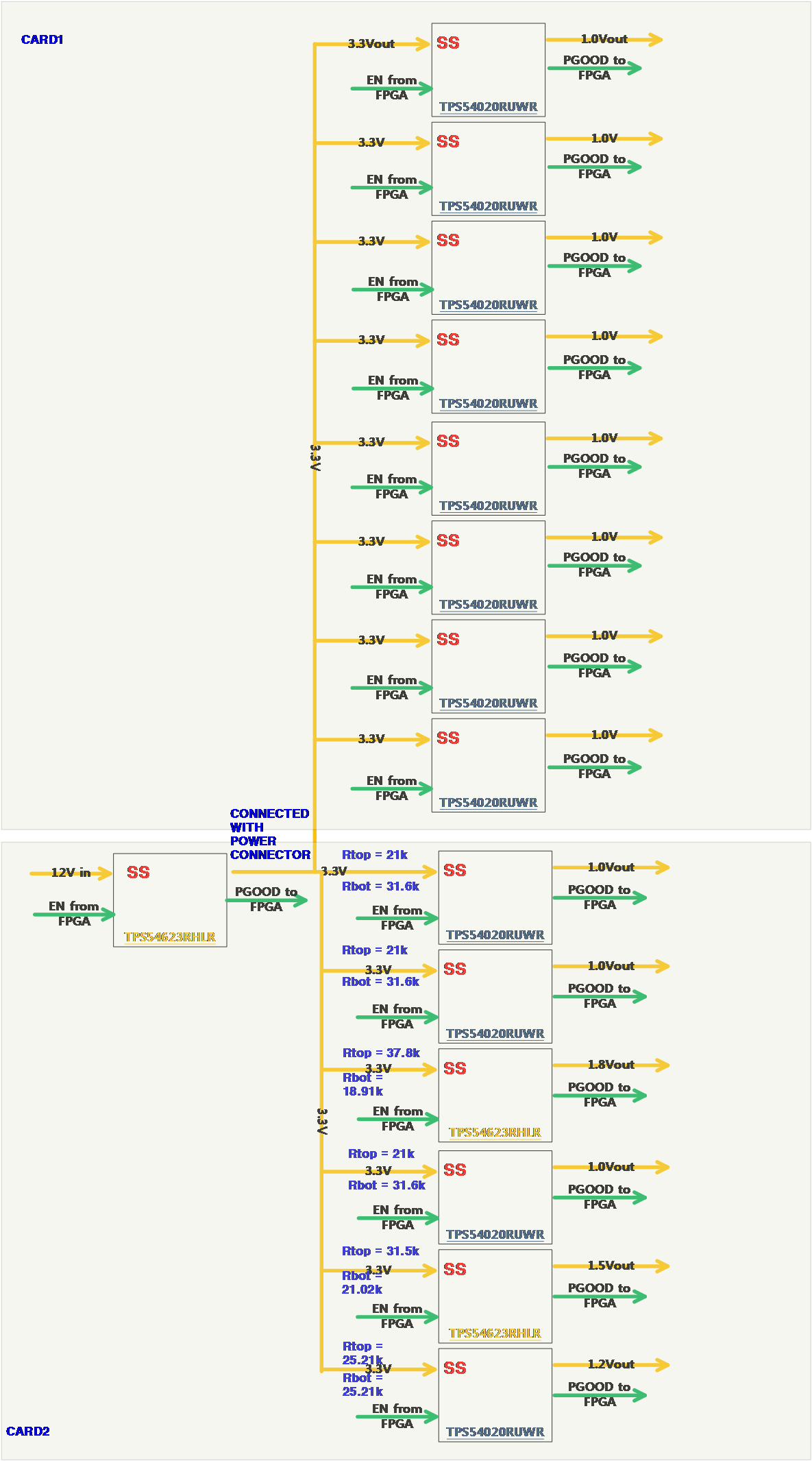
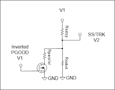
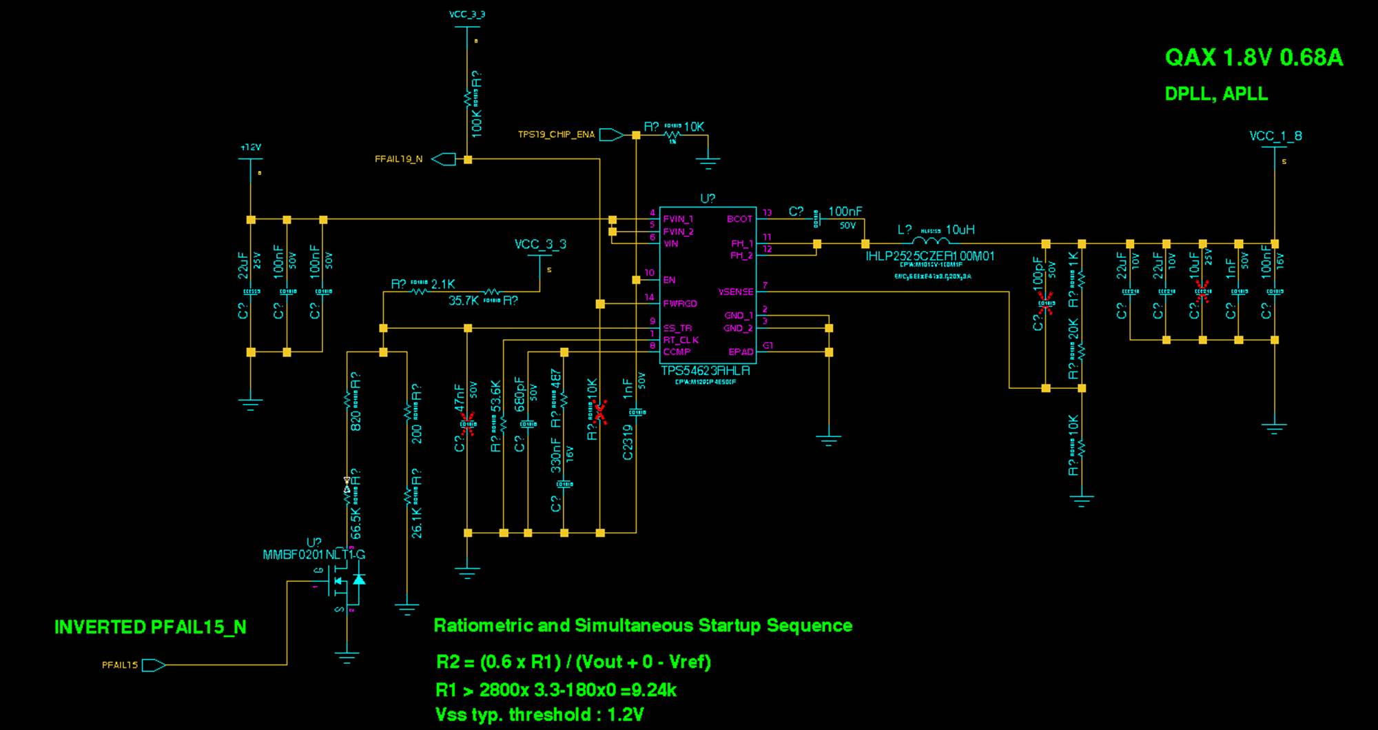
1. Please review and confirm our schematic.

0827.TI power review.pdf

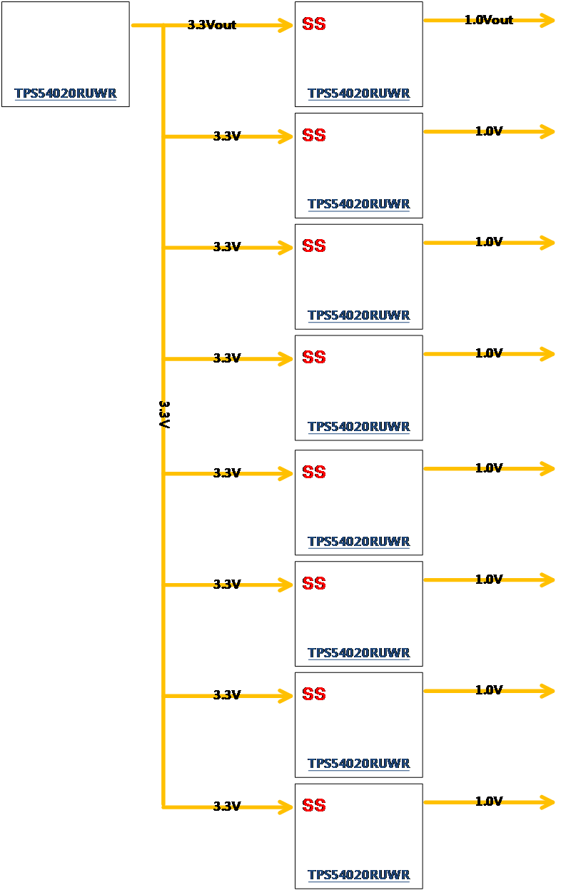
2. Is it possible to design with following structure? (8 parellel TPS54020s)

thanks,

TS

  • Hi TS,

    Overall I do not see any issue with what you are planning to do but there are a few things I need to confirm.

    1. Could you clarify if you plan to power 8 different 1.0 V loads or will all of the 1.0 V outputs be connected in parallel? I do not see any problem with the current configuration if you plan to have 8 independent 1.0 V outputs. If you need to parallel them, you would need something added to this to ensure proper current sharing.
    2. How closely do you need the 1.0 V outputs to track each other during startup? There would be some variation in the output ramp due to circuit tolerances in the VSS to VFB offset and the ISS current.
    3. Make sure you use the corrected equation suggested by John. It should be Vout2+deltaV, not Vout2*deltaV. Unfortunately sometimes these mistakes happen when the datasheet is converted into pdf and they are very easy to overlook.

    Hope this helps.

    Anthony

  • Hi Anthony,

    thanks for your answer.

    1.Could you clarify if you plan to power 8 different 1.0 V loads or will all of the 1.0 V outputs be connected in parallel? I do not see any problem with the current configuration if you plan to have 8 independent 1.0 V outputs. If you need to parallel them, you would need something added to this to ensure proper current sharing.

    -> Thanks for the review. 1.0V outputs are independent, there’s no need for me to use current sharing.

    2. How closely do you need the 1.0 V outputs to track each other during startup? There would be some variation in the output ramp due to circuit tolerances in the VSS to VFB offset and the ISS current.

     -> How much do VSS to VFB, ISS affect on the variation in maximum?

    Only thing I need is 1.0V outputs tracking 3.3V and variation among 1.0V outputs ramp-up would be less than 2.5msec.

    Do you suggest 1.0V outputs tracking each other including tracking 3.3V?

    3. Make sure you use the corrected equation suggested by John. It should be Vout2+deltaV, not Vout2*deltaV. Unfortunately sometimes these mistakes happen when the datasheet is converted into pdf and they are very easy to overlook.

         -> I confirmed the equation in the TI website. I have applied the correct equation which you have suggested.

    thanks,

    TS

  • Hello TI,
    Please answer for my question of above item 2.
    My question is whether TI device can track 1.0V during 3.3V tracking.
    And if 1.0V variation(circuit tolerance) is less then 2.5ms, then it would be ok at our system i think.
  • Hi TS,

    I apologize, I must have overlooked your question in the second item. I have two more questions with some comments before I can answer this.

    Questions: How closely do you need the 1.0 V to track the 3.3 V?

    Comments: When the correct equation is used (Vout2 + dV) the top resistor for the divider from the 3.3 V to the SS/TR pins is 21 kΩ. This gives an offset between the 3.3 V and 1.0 V output of nearly 0 V. When the max values for the Vssoffset and Iss from the electrical specifications table are used in this same equation, the offset becomes -0.3 V. This means the 1 V output may lead the 3.3 V output by 0.3 V. Using the min value of Iss and the typ value of Vssoffset shows that the 1 V output could lag the 3.3 V output by 0.3 V.

    Question: What SS time will you use for the 3.3 V output?

    Comments: As long as the startup time for the 3.3 V is in a normal range, it should not be a problem to have all 1.0 V come up within 2.5 ms. For example a 5 ms startup time could work because 2.5 ms is only 50% of the startup ramp time.

    Do you actually need the outputs to track or is really only important to make sure a specific startup sequence is met? If only the sequence is important, using PWRGD of the 3.3 V output to enable the 1.0 V outputs would greatly simplify this.

    Best Regards,
    Anthony

  • Hi,

    I reply on your questions below.

    Questions: How closely do you need the 1.0 V to track the 3.3 V?

    Comments: When the correct equation is used (Vout2 + dV) the top resistor for the divider from the 3.3 V to the SS/TR pins is 21 kΩ. This gives an offset between the 3.3 V and 1.0 V output of nearly 0 V. When the max values for the Vssoffset and Iss from the electrical specifications table are used in this same equation, the offset becomes -0.3 V. This means the 1 V output may lead the 3.3 V output by 0.3 V. Using the min value of Iss and the typ value of Vssoffset shows that the 1 V output could lag the 3.3 V output by 0.3 V.

    -> 1.0V should track 3.3V with zero delay. (See the graph below)

    Question: 
    What SS time will you use for the 3.3 V output?

    Comments: As long as the startup time for the 3.3 V is in a normal range, it should not be a problem to have all 1.0 V come up within 2.5 ms. For example a 5 ms startup time could work because 2.5 ms is only 50% of the startup ramp time.

    Do you actually need the outputs to track or is really only important to make sure a specific startup sequence is met? If only the sequence is important, using PWRGD of the 3.3 V output to enable the 1.0 V outputs would greatly simplify this.

    ->

    As I commented earlier on the graph, the slope of start ramp time for 3.3V should be 0.2V/msec. (See the graph below)
    So,
    the total of start ramp time for 3.3V will be 16.5msec.

    The reason that I chose for
    ratio-metric and simultaneous startup sequence circuit design is to track 3.3V and to make 3.3V and 1.0V with zero-delay at the same time.
    IF I can meet those two conditions, any circuit design is fine for me.
    please advise.


  • Hi TS,

    Zero delay is not possible with this circuit. There will always be some variation in the startup due to tolerances in the SS current and the offset from SS to FB. Some 1.0 V outputs could lead the 3.3 V and some could lag the 3.3 V.

    Where does this zero delay requirement come from? Is there a maximum limit specified for the voltage difference between 1.0 V and 3.3 V?

    Anthony

  • I double checked my calculations by coming up with an equation to estimate the 1.0 V output based on the 3.3 V output during the startup ramp. This equation is derived by simply summing the currents into and out of the SS/TR pin node. Equation is below. This equation only works for the case of Vout2 = 1.0 V. Also this equation is only valid for Vout1 up to ~1.0 V because the max voltage at Vout2 is the regulated 1.0 V.

    If the 21k and 31.6k SS/TR resistors suggested earlier by John are used, then the 1.0 V output could lead or lag by ~30 mV. For example, when the 3.3 V output is at 0.1 V, the 1.0 V outputs may be 0.13 V or 0.07 V. This same offset would remain through the entire startup ramp. Will this much voltage difference be acceptable for what you are powering?

    Previously I was using Equation 5 incorrectly which incorrectly suggested a larger difference.

  • the 21k and 31.6k SS/TR resistors suggested earlier by John are used, then the 1.0 V output could lead or lag by ~30 mV


    I think that would be acceptable for the 1.0V outputs.

    1.0V Core voltage should ramp up earlier than the other voltages that runs in the whole system. (3.3V, 1.8V, 1.5V).

    (IF 1.0V core voltage lags 3.3V outputs more than 2.5msec,. It will be a problem.)


    Question)

    I’d like to use the other TI powers in the other kind of system with similar structure.

    Would you like to cross-check Rss values that I calculated in the structure below?

    And how much variation will occur among them?

    (it is also individual outputs, so there is no need to current sharing)


    <tracking 3.3V with zero-delay (the variation should be less than 0.5msec, which means outputs lag or lead 3.3V in 0.1V max) >

    TS

  • Hi TS,

    Just a couple comments.

    To have the 3.3 V track the other 3.3 V rail, I suggest that you instead connect the SS/TR pins in parallel. Both parts should have a local SS/TR capacitor. The capacitance would also need to be ~2x because the two SS/TR current sources would be placed in parallel.

    Will you be using the PGOOD/PWRGD outputs in your design? The output of the 1.8 V rail will not be valid because the SS/TR voltage will not reach the typical 1.2 V, 1.4 V max threshold. An external circuit work around is possible if you need this signal to be valid. Let me know if you need this in your system and I will provide a more specific suggestion.

    Anthony

  • Dasan networks_card1_TPS54020_review.pdf

    Dasan networks_card2_TPS54020_TPS54623_review.pdf

    I use power good signals individually which are all connected to FPGA.

    FPGA will control with PGOODs. To make sure power is turned on before running through any kinds of data in our system.


    1.

    My apologies to incorrect diagram. Here is correct version below,

    I should have explained you that there are two cards and all the power rails on the two cards should track 3.3V with zero-delays. (ramp up 0.2V/msec)

    According to the diagram, I assume that I don’t need 3.3V parallel connection you suggested .


    Is this structure still work without any problem?


    2.

    BUT I don’t get what you said about extra work-around circuit on 1.8V regulator.

    (à the SS/TR voltage will not reach the typical 1.2 V ) Is it because Rss values on 1.8V block came from EQ5 is something wrong?

    If 1.8V rail SS voltage causes that kind of problem, why doesn’t 1.5V rail have that kind of problem.? 1.5V rail uses same part with 1.8V rail. (which are, TPS54623 )


    I have attached the whole circuit schematics of TI powers that I designed.

    Would you review the schematics that is designed what I intended?


    3.

    3.3V ramp-up time is very important. (ramp up 0.2V/msec, 3.3V rail will reach to the 3.3V level in 16.5msec)

    When you review, please see the value that I chose for Css in the 3.3V rail/

    4.

    I can see there is some limit on soft start time in Designer tool. (I couldn’t find in the datasheet though.)


    TPS54020 : max soft start time 25ms

    TPS54623.: max soft start time 10ms


    Is it possible to use TPS54623 for 3.3V rail to make soft-start in 16.5msec ?

    Is it possible to track 3.3V with same soft start time(16.5msec) for other voltage rails that are using TPS54623 ?


    thanks,

    TS

  • Hi TS,

    1. Ok, got it now. I don't see any issue with this structure.

    2. The reason the 1.8 V needs this extra circuit but the 1.5 V does not is the differences in the resistor divider at the SS pin.

      1. For the 1.5 V, the divider is 30.9k and 21.01k. When the 3.3 V is in regulation the voltage at the SS/TR pin is ~1.336 V. This is above the 1.2 V typical threshold so PGOOD will go high.

      2. For the 1.8 V, the divider is 35.7k and 18.909 k. When the 3.3 V is in regulation the voltage at the SS/TR pin is ~1.143 V. This is below the 1.2 V typical threshold so PGOOD will never go high.

      3. To work around this you can add an NFET which changes the SS divider for the 1.8 V based on the state of the 3.3 V PGOOD. See image below and description of how this works. This circuit assumes you have a way to invert the PGOOD of the 3.3 V rail.

      1. Rsstop remains the same.
      2. During startup, when the 3.3 V PGOOD is low, the MOSFET is on so the combination of Rssbot and Rparallel should equal the value calculated in the datasheet equations.
      3. When the 3.3 V PGOOD goes high the remaining divider should pull the SS/TRK voltage to just above 1.4 V.
      4. For the 1.8 V the two bottom resistors are calculated as:

        Rssbot = Rsstop*1.4V/(V1-1.4V)
        Rparallel = Rssbot*Rssbotstartup/(Rssbot-Rbotstartup)

        Where:
        V1 = 3.3 V rail for your application
        Rssbotstartup = the resistance calculated by the datasheet equations, 18.9 kΩ in this application.

      5. Using these two equations I calculate that you will need:
        Rssbot = 26.3 kΩ
        Rparallel = 67.3 kΩ


    • There is no problem using a 16.5 ms soft start for the TPS54623 and you can use the equation you showed from the datasheet to select the appropriate capacitor. This is just a random limitation they decided to use in WEBENCH.
  • Hi Anthony,

    Thanks for your support.


    However, total value of Rsstop for 1.8V regulator is not 35.7kohm, but it is 37.8kohm in the previous schematics. (Since R2 = 18.9kohm, R1 should be 37.8kohm because of EQ5)

    Anyways, even though R1 = 37.8kohm, the voltage at the SS/TR pin will be ~1.356 V. I don’t see this would be a problem for PGOOD to go high.

    Based on work-around solution that you have suggested, I modified 1.8V regulator like the below. (Please review the circuit below)

    And please let me know if you have found a rest of circuits.

    thanks,

    TS

  • Hi TS,

    What you have now looks good.