This thread has been locked.

If you have a related question, please click the "Ask a related question" button in the top right corner. The newly created question will be automatically linked to this question.

TPS61175: Is it recommended to use snubber circuit to reduce noise?

Part Number: TPS61175
Other Parts Discussed in Thread: TPS61088

Hi,

I am designing a 4 layer board with a TPS61175 boost converter (10V to 22V, 350mA load), the board also has an RF transceiver at 120Mhz (not part of the load).  I'm trying to reduce the interference of the boost converter on the transceivers performance.  Would it be worth considering the inclusion of an RC snubber between the switching node and ground to reduce harmonics, or is it not recommended with TPS61175?  

Also, would separate ground planes a good idea? 

Regards

Matt.

  • what is the location of the RF transceiver? sch location? PCB location? their GND connected together? where is the power supply of the RF transceiver come from?
    Generally, TPS61175 should be OK for this application but need be careful on the layout.
  • Hi Helen

    The TPS61175 is used as a constant current source for LEDs, I will filter the output with ferrite bead and small caps.

    The RF transceiver and TPS61175 are well separated by 60mm.  The 12V battery connection for+ and -(gnd) are located at the TPS61175 inductor, at the edge of the board.  The RF transceiver is powered from 3.3V bus, supplied by LDO also connected to 12V+ rail.

    Would filtering the 12V supply to the 3.3V LDO with a ferite bead and small caps help reduce any noise generated by the switcher on its input side? Or would it be better to put a ferrite bead between the 12V+ and the switcher's inductor which would also filter any RF that would radiate on the battery supply wires?

    Would it be a good idea to separate the ground planes, and just have the ground connection at the 12V- battery connection at the very edge of the board?  Or is this unnecessary as the components are well seperated, and none of the current flowing in the switcher circuit flows to the other side of the board where the RF transceiver is located?

    Is it not recommended to use RC snubber to slow slew rate and reduce harmonics? If so what values? 

    Am I right in saying that the interference from the switcher is going to be due to harmonics from the FET and doesn't really have anything to do with the p-pV at the switchers Vout, as the switcher is not supplying the RF transceiver? In which case the lower the frequency of the switcher the less RFI?

    Would it be best to design with the slowest switching frequency?  Webbench suggests solutions at 173Khz with 200mVp-p, or 665Khz with 80Vp-p, which is likely to give the better solution regarding RFI?  At the lower frequency of 173Khz, a snubber circuit would have less of an effect on efficiency.  

    Do you think I should design in component places for a snubber? I can always leave them empty if they are not necessary.  Or Will the TPS61175 not tolerate a snubber?

    Regards

    Matt.

  • Hi Matt,

    Good quetion.

    Here's my reply:

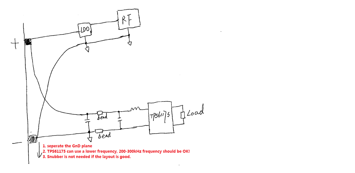
    1. The GND plane must be seperated.

    2. TPS61175  can use lower frequency , 200-300kHz is OK, lower frequency means lower radiation energy.

    3. Snubber is not needed if the layout is good. But you can keep it if have the space.

    4. keep some space from the TPS61175 and inductor to the RF receiver.

    I draw a draft pcb layout diagram for this application.  Please check the below picture.

  • by the way, could you please send the detailed application information for us? Like in what kind of equipment? Which company?Volume? This is also one  of our work becuase we need to collect customer informaiton:)

    You can send the information to me by email, my email address is helen-chen@ti.com

  • Hi Helen,


    I replied to your email with my company and project details, I hope you got it.

    I have another question regarding Webench.  When I put in my parameters of Vin(min)10V, Vin(max)14V, Vout 22V, load 0.35A and turn the dial to max efficiency, the Visualizer shows the solution using TPS61175 at 173Khz, but the data sheet says a minimum of 200Khz.  If I click on OPEN DESIGN the schematic shows Rt(frequrncy resistor) of 576K. Is this the correct value for 200Khz or is it OK to operate at 173Khz as suggested in webench solution?  If I click on USE ADVANCED OPTIONS and then tick USER PREFERRED FREQUENCY (200Khz) none of the component values or parameters are changed.


    Also, in your drawing you show a resistor between the IC input and ferrite bead/capacitor.  Is this resistor part of the filter, or is this infact the inductor? If it is a resistor, what value should it be? I imagine the capacitor values, either side of the beads, will be in the order of 1000pF which gives low impedance between 50 - 250Mhz, or should I be using something larger?

    Thanks.

  • Sorry for the late.

    The minimum operation frequency of TPS61175 can be typically 200kHz, minimum value can be reach 150kHz. I'll check with the Webench team how did they get 173kHz. But this is value is very near to the actural value. There should be no big error.

    What is the RFI operation frequency range? The bead's best operation frequency range should conver this range.

  • That is boost inductor, not resistor. Sorry for the confusion.for capacitor in front of and behide the beads, please use a 10uF capacitor in parallel with a 1-10nF cap. only one 1nF cap is not enough.

  • Thanks Helen, your awesome!
  • TPS61175 constant current LED driver.pdfHi Helen

    Did the Webench team get back to you regarding their recommendation of frequency resistor 576K at 173Khz?

    Also please see attached schematic of my application.  Rather than using a resistive divider to set Vout, I am taking the FB upstream of a variable resistance for constant current control.  Could you recommend values for Rcomp and Ccomp?  It's way beyond my comprehension.

    Also do you think the EMI filter of ferrite bead plus 1nfCap will cause resonant peaking that will require damping? See notes on schematic.

    Thanks

    MattTPS61175 constant current LED driver.pdf

  • I'll push the Webench team to give the feedback to me soon! Please wait in patient. But their lowest frequency should be no big problem, it is around this  value.

    I'll study the sch ASAP!

  • FB3 and C21 is not needed in the schematic. They are not fittable in that location. you can remove them from the schematic.

  • Hi Helen,

    I need to filter the output for EMI/RFI . The load LEDs are very near to the antenna of the radio which operates at 120Mhz. Boost converters typically emit a lot of noise in this VHF region. Is it not possible to compensate the boost converter for stability with this filter on the output? I don't need a rapid response to transients, just that the converter doesn't fall over when transients occur.

    Without this filter how am I going to eliminate the RFI?

    Regards

    Matt.
  • The radiation can be directly coupled to the receiver through air. Therefor the LC filter at the output only benefit the conduction(not sure, based on the value), it will not benefit the radiation.
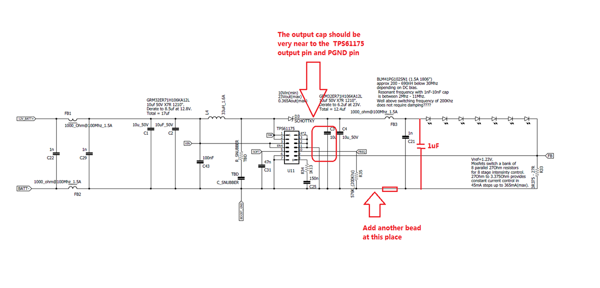
    To reduce the radiation, you need to make the output load, that is the LED load loop as small as possible. (From the TPS61175 output, output cap, to LED, then return) . And this loop should be far away from the RF receiver. For the directly coupling radiation, filter is not effective. And the LC filter put in this place may even cause the stability issue.
    I remember in your last post, you mentioned the TPS61175 is at the side of the board. And it has distance with the RF receiver.  Could you also make the LED has a distance with the receiver. But most important of all, you need to optimize the loop, you need to put the output cap very near to the output pin of TPS61175.

  • Chang the LC filter to LCL filter will help for the radiation. please check the following picture . But it still greatly depend on your layout.

  • Thanks Helen, once again your super.

    I've incorporate those extra component into the design.

    Are you able to give advice on what the values for Ccomp and Rcomp should be for max stability?

    Regards  Matt

  • Hi Helen,

    A question regarding the placement of the bead between the load and ground. Should the filter caps C21(1nf) and your 1uf cap decouple straight to ground or should they go to ground through the bead as in your revision to the schematic?

    Regards Matt.
  • From the radiation EMI point of view, they should be placed according to my sch. Because this is mainly for the common mode noise reduciton, CM noise is mainly focus at the 30-300MHz range. But from the control point of view, as it detects the FB voltage, so the bead resistance should not be too big. 100 ohm bead is OK, the voltage drop of the 1000 ohm bead is much bigger than that of the 100 ohm bead. which may effect the LED current detection.

    What I did before is just add the LCL bead directly before the output load. But your design combines FB, so you need to check carefully if it is OK with this configuration. If the bead at the return path (between load and GGND)effect the LED current, then you may have to remove it.

    And the key point is that make the output loop as small as possible, make the output load trace as short as possible.

  • not sure what kind of effect the output bead will have? because it is not inductor.  If not consider the bead. Rcomp=511 ohm, Ccom=1uF. Cp=100pF(Cp is from the COMP to GND) is fit for this application. Since for the LED applicaiton, response time is not so important.

  • 7144.TPS61175 constant current LED driver.pdfHi Helen,

    Thanks for calculating the compensation components for me.

    I didn't think the the bead to ground would cause problems for FB pin as it is only 90mOhm for DC.

    I didn't consider that the FB might be sensitive to signals at frequency however.

    I have moved the bead upstream of the FB resistor.  How does it look to you?

    Thanks again.

    Matt.

  • Move the bead upstream of the FB resistor doesn't help the common mode noise. Not suggested, but you can try it.  

    Radiation EMI is a complex mechanism, layout is even more important than filter. the LED is near the atenna, really don't know what will happended. Did you shiled the LED?

  • Hi Helen,

    Yes its a dark art, at least for the uninitiated. 

    I'll leave the circuit as is then, with the bead on the ground side of the FB, and I'll see how I get on. 

    I read your SLVA790 "Reducing radiated EMI in TPS61088 Boost converter", which is the most useful reading I found on the net.  

    In that article you suggest a 1uf high frequency Cout closest to the power ground.  My layout for the TPS61175 is the same as the data sheet, would you recommend I put an 0402 0.1uf or an 0603 1uf closest to the ground pins? (even though it moves the bulk 10uf caps further away)?

    Thanks again for your support.

    Cheers

    Matt.

  • Both the 0.1uF and the 10uF cap should be very close to the output pin. Because the DM ripple will become the CM noise during transmission. then it will be even hard to be filtered.