Hello,
I am working on a design using an LM3150. I've attached schematic/layout and a scope capture below, as well as the webench design report. I'm assuming I have an issue with my layout, but I would like some help before I spin another revision with some changes.
The design is supposed to use a ripple injection circuit and the BOM matches the webench report. However when apply any sort of load, the output regulates up to 7-8V, becomes incredibly noisy and I can hear the regulator. I can reset the regulator only by powering it off completely. What I have found is that the only way the design works is if i completely remove the injection circuit. I get a proper 5V output but there is significant ripple. I'm assuming there's an issue with my layout due to the fact that the switching node is noisy as well.
I have also tried using the same design with just a Cff cap, and a 68uF instead of 100uF output cap (as per webench) and have similar issues.
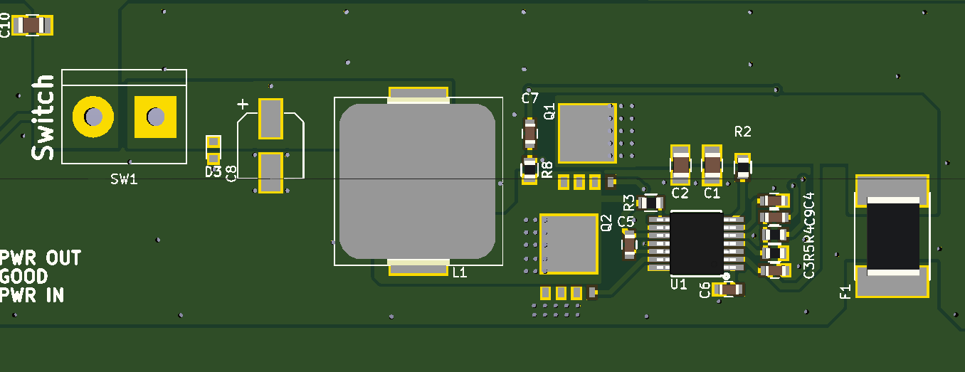
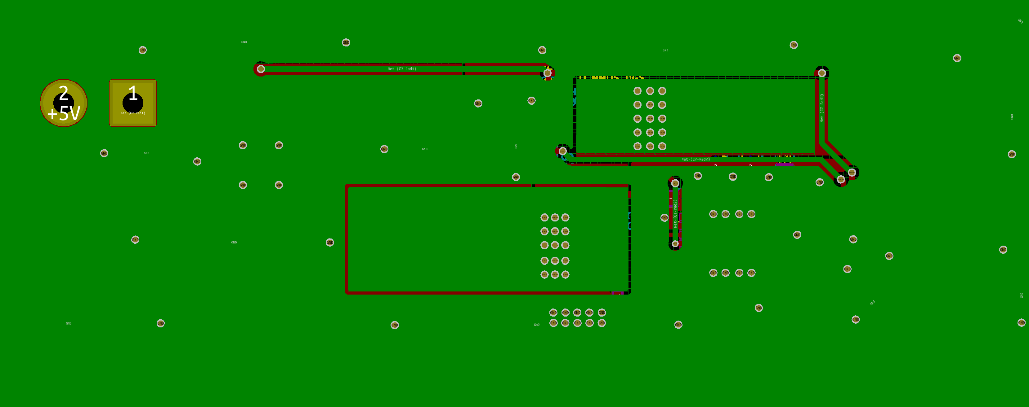
Schematic:

Layout:

Scope capture (no injection circuit):
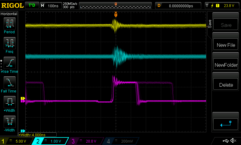
CH1: Vin
CH2: Vout
CH3: SW node
I'm going to remove the ground pour under the inductor and try and shift the FET's and inductor in a bit closer towards the IC to try and shorten trace/pour lengths. I'm also assuming my connection from the switch node to the IC is mediocre and I want to improve that.