This thread has been locked.

If you have a related question, please click the "Ask a related question" button in the top right corner. The newly created question will be automatically linked to this question.

TPS55332-Q1: TPS55332-Q1 does not up-convert 3.3Volts to 40Volts

Part Number: TPS55332-Q1

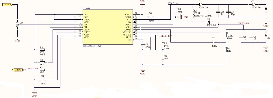
Dear Sir/Madam, I have made a PCB based on the application note found for the TPS55332-Q1 part.

I am trying to up-convert an input voltage of 3.3V to 40V. Please can you go through the attached schematic and point out any issues?

I have simulated the circuit components using TINA and managed to confirm functionality, but in reality the regulated output voltage is 2.4V rather than 40V.
  • TI engineer is working on this request. He will reply as soon as possible.
  • Hello Nishanth,

    Please provide the maximum output current? This is needed to check the design.

    It sounds the like device might not be enabled since the input voltage is 3.3V and the output voltage is 2.4V. Please ensure that the EN pin is pulled high.

    Thanks,

    Garrett

  • Hello Garrett,

    I need to draw a maximum of 3.2mA from the output port J3 on the diagram.

    To check the operation of the platform, I raised the Vsupply to 11V, and noticed that the output voltage across J3
    was measured correctly to be 40V (no load). However, the Vsupply was drawing a maximum of 77mA of current.
    When I started to lower the Vsupply towards 3.3V, I noticed the current drawn was increasing from 77mA to 150mA
    from the Vsupply (J1).

    Finally, I noticed that Vin was 40V, how can this be? When I removed the inductor (22uH) I noticed that VIN and EN
    followed Vsupply (J1), and placing the inductor from Capacitor C2 to Anode of Q3 doesn't improve the issue as VIN
    on pin 19 was measured to be 40Volts.

    I have checked the PCB for shorts but not been able to find any. Can you please make a few suggestions why
    VIN is measured at 40Volts when Vsupply is 11Volts (J1)?

    Best Regards,
    Nishanth

  • Dear Garrett,

    I am drawing a maximum of 3.2mA via J3 the output port, and feeding 11Volts at 77mA from the Vsupply port J1. The interesting aspect is the output voltage is 40Volts as expected. However my VIN pin 19 on the IC appears to be 40Volts too, considering I am only supplying 11Volt?

    I have investigated my PCB for shorts and cannot find any, can you suggest how VIN raises to 40Volts from a Vsupply of only 11Volts?

    Thanking you
    Nishanth
  • Hello Nishanth,

    Can you please clarify what were jumpers J1 and J3 are located? They don't not appear on the schematic that you provided.

    Also please not the TPS55332 requires about 3.6V to start-up initially. This is shown in section 7.2 of the datasheet.

    Thanks,

    Garrett
  • Hello Garrett,

    J1 and J3 are to the right side of the diagram. J1 is the input close to diode Q1,
    whilst J3 is also located to the right of the diagram. J3 is close to capacitor C6.
    This is where the output is taken.

    Yes, I am aware that 3.6V is needed to start up the converter initially. so I do provide
    the input with more than 3.6Volts.

    Can you please advise if the power inductor I am using 22uH, is suitable for delivering
    a 3mA output current?

    Best Regards,
    Nishanth

  • Hello Nishanth,

    Please note that there should be a diode between the VIN pin and the voltage of the external supply. This is similar to D1 on the TPS55332 evaluation model. This due to how the internal LDO operates. 

    For the inductor, select a component that has a saturation current of higher than 5.7A as this is the internal current limit of the TPS55332. The inductor that has been selected has a saturation current of 2.3A.

    Thanks,

    Garrett