This thread has been locked.

If you have a related question, please click the "Ask a related question" button in the top right corner. The newly created question will be automatically linked to this question.

TPS650250: Clamping Circuit issue with TPS650250.

Part Number: TPS650250
Other Parts Discussed in Thread: TLVH431, TR100

Hi,

Our customer system is using TPS650250 PMIC with AM335x.
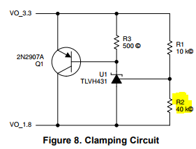
The Clamping Circuit is also used as per the suggestion in the manual (SLVU731A).

But, there is an issue in power-up sequence after adding this Clamping Circuit.
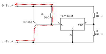
During power up, after the 1.8V line is powered up, there is a short voltage(0.6V)
induced into the 3.3V before 3.3V line is powered up as shown below.


Please let us know is this a problem in the recommended circuit
and will there be any issue on the power up sequence.

Best Regards
Kummi.

  • Kummi,
    I am passing this to the product specialist. Someone should get back to you soon on this.
  • Kummi,

    Why did you modify the clamping circuit's R2 value? 

    Your circuit:        R2 = 22k

    SLVU731 circuit: R2 = 40k

    You should review the math that you used to modify this circuit, because changing R2 will impact the characteristics of the TLVH431 clamping circuit.

    I cannot tell you if this is a problem for sequencing because I cannot see any other rails in the system. Sequencing, by definition, is the order in which the voltage rails power-up or power-down. The "step" in the power-on of DCDC3 will only cause a problem if it changes the sequencing order.

    Please provide a scope shot showing the power-up sequence and power-down sequence for DCDC1, DCDC2, DCDC3, and LDO1 (4 channels).

    If possible, you should also take a scope shot of the power-down sequence without the clamping circuit.


    As it says on page 10 of the App Note SLVU731, the clamping circuit is an attempt to meet the requirements of the AM335x datasheet:

    "Reading the datasheet for the AM335x, (SPRS717), and the challenge when ramping down VDDS and VDDSHVx [1–6] simultaneously is obvious. 'If it is desired to ramp down VDDS and VDDSHVx [1–6] simultaneously, it should always be ensured that the difference between VDDS and VDDSHVx [1–6] during the entire power-down sequence is < 2 V. If this is violated it can result in reliability risks for the device.' This only refers to 1.8-V VDDS and 3.3-V VDDSHVx rails. The worst-case scenario of this issue is the 3.3-V rail remains high possibly because of large output capacitance or no load being present on the output while, the 1.8-V rail ramps down quickly such as if it were fully loaded."

    You only need the clamping circuit if there is so much capacitance on DCDC3 that the difference (VDCDC3 - VDCDC2) > 2V

    If you do not measure this >2V delta without the clamping circuit, then it is not necessary in your design.

  • Also, what is the Part # for the transistor you are using?

    The screen shot you took just says TR100, but this is a designator and I need to see the part number.
    The SLVU731 App Note clearly shows a 2N2907A PNP belchip.by/.../28790.pdf

    Since the clamping circuit is designed specifically for this use case, I do not recommend any change in values for resistors or semiconductors.
  • Hi Brian,

    Thank you for the details.

    The resistor R2 = 22k is decided considering the overall worst case values.
    But, we believe this resistor is not the root cause of this issue.
    As shown below it seems this circuit allows current from 1.8V line to 3.3V line
    through the transistor and the resistor R3 as soon as 1.8V line is powered up.
    Could you please re-check if "Figure 8. Clamping Circuit" is the recommended circuit?


    Regarding the transistor, PNP transistor (part number:2SAR553PT100) is used.
    and I belive it is similar to the part number on the recommended circuit(2N2907A).

    Actually, the customer has tried to remove the transistor and there was no
    such issue without the transistor. We assume this issue solve by removing the Clamping Circuit.
    But,we want to follow the recommended design on the appli note.

    If possible can I send you the scope shot of the power-up sequence through
    message, please accept my friendship request.

    Best Regards
    Kummi

  • Kummi,

    Since I did not design this clamping circuit, I would need you to re-test with the recommended value of R2=40k to determine if this has any impact on the behavior you are observing.

    I cannot accept a friend request just to accept these scope shots. It does not improve the process of sharing info. If you cannot attach the scope shots here, you will need to send them to your local sales representative at TI so that he/she can begin a separate discussion with me over e-mail.

    Finally, if the rise in voltage on the 3.3V rail during the power-on sequence did not immediately cause a problem in your system then I do not expect it to cause any problems in the future. If the sequence order is still intact, then this minor deviation on the 3.3V rail will have no impact.
  • Brian,

    Thank you for the information.
    I have contacted local TI.

    With regards to the "R2=40k", we believe that R2 is not the root cause.

    I just wanted to make sure if TI has already tested with the Figure 8. Clamping Circuit.
    The Appli Note(SLVU731A) don't have the Scope shots of Power-Up sequence with
    Clamping Circuit, it has only power-down Scope shots.
    Could you please check if TI has Scope shots of Power-Up sequence.

    We understand there is no issue as such with this glitch in the power-up sequence
    but we would like to know what could be the possible cause.
    Except some parts like Transistor this application use all TI products.

    Best Regards