This thread has been locked.

If you have a related question, please click the "Ask a related question" button in the top right corner. The newly created question will be automatically linked to this question.

TLV62569: Design check for 3.8V-5V input, 3.8V output

Part Number: TLV62569

Hello there,

I have the following design:

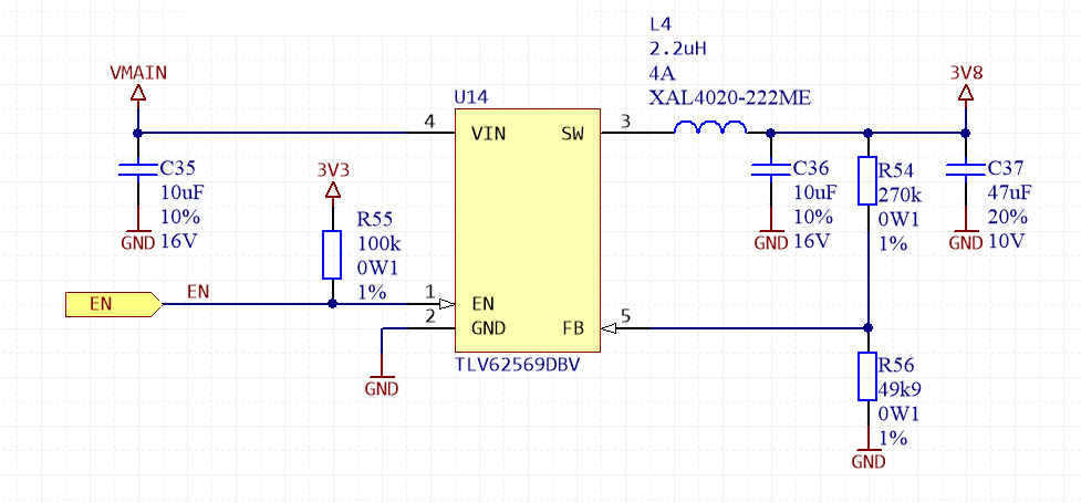
VIN can vary from 3.8V to 5 V. At the output I need a stable 3.8 V with 2A peak currents. This buck converter is very convienet for me as its very space sensitive and has comfortable package. It is a bit small however and I am wondering either it can really supply up to 2 Amps. Could I ask for a peer review of the schematics? I would appreciate all help.

  • Hello Lukasz,

    It's a pleasure to help!

    I can see you followed our datasheet's recommendation on the input cap in order to reduce input voltage ripple. I would say that the output caps are also fine, considering the capacitance derating. Just be sure that the total effective capacitance is between 10uF and 46uF.

    From your feedback divider I can calculate an output target of circa 3.85V and I see you are using 1% tol resistors. If you'd like to get the rid of those 50mV I would suggest to redesign the feedback devider. You can use our Voltage divider calculator which takes into accout standard resistor values fro E24 and E96 series. Something I think you would enjoy is also the reading of the application note SLYT469 on the use and design of reactive feedback devider.

    The max recommended operating current in datasheet is 2A. It also recommends to properly manage the thermal dissipation in order to keep the junction temperature under the max recommended of 125 degC. Your dissipation pads must have a thermal resistance small enough to dissipate the heat generated by Joule effect in your converter. For more details on how to use the thermal parameters, see the application notes SZZA017 and SPRA953

    Last but not the least, mind that the most important part of a DCDC switching converter is the electrical layout. A general rule is that the paths of the switching currents must be as short as possible, in order to limit the stray inductances which cause excessive ringings, conducted and radiated noise. When you'll be at that point you may simply have a look at the datasheet's layout guidelines at section 10 and a read to this.

    Enjoy your design,

    Emmanuel