This thread has been locked.

If you have a related question, please click the "Ask a related question" button in the top right corner. The newly created question will be automatically linked to this question.

BQ77PL900: Balance Problem

Part Number: BQ77PL900

Hi, 

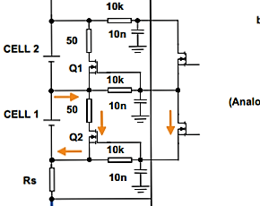
I would like to ask a question about bq77pl900 external cell balancing problem.I have external FET configuration for 6 series cell as shown in the picture below.

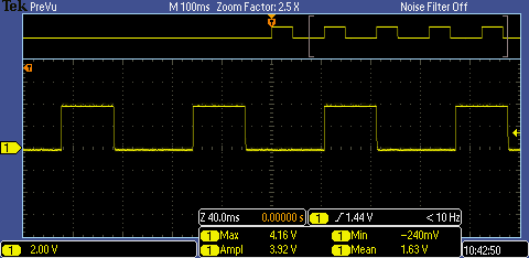
Here my problem begins.After one cell reaches OV level , charge stops and cell balancing starts.If that balancing starts at first cell (in this picture CELL 2) i can get battery voltage around 4,01V at balance resistor(50ohm).Until this moment everything is just perfect.Whenever cell balancing shifts to other cells for example 4 th cell from top, voltage at balance resistor decreases to max 1V. The picture of scope has taken while first cell started to balance.But the rest of balance resistors voltages are not like this. They are not balancing correctly.How can i solve this problem?

Thanks.
   

  • Hi Metin,

    Be sure the view of the voltages is not being limited by the equipment such as a common mode limit.  You may want to explore the movement of each pin during balancing with single ended probes to determine what is not working properly.  For example if VC10 and VC11 pull together to some value when balancing cell 1, VC5 and VC6 should similarly pull together when that cell balances.  If they pull together but stay toward the VC6 value the FET may not turn on much and you might see a low voltage on the balance resistor.

    You might check the specs of the balance FETs or variation of the FETs.  If balancing at 4V/cell and the VCx signals pull completely together there is only 2V Vgs available to the FET.  Since there is an internal resistance in the 'PL900 the pins won't pull completely together and the available gate voltage will be lower.  You would like the FET to have a specified RDSON at a the available voltage or lower, or consistent performance below the spec.

    If the VCx signals are not moving symmetrically check for connection problems or damaged components. The schematic shows the 10nF caps to ground on the inputs.  During cell connection the caps will try to hold the voltage at ground before they charge, this can stress both the FET gate and the input pins of the bq77PL900.  The differential caps shown in the page 6 diagram help avoid that condition.  In some cases you may need to protect the external FET gate with a zener and resistor, see figure 6 of slua749 as an example.  Although that diagram is for a different device the same issues can occur on an external balance circuit.

  • Hi,

    Firstly thanks for reply. Sorry for the old schematic which i sent you yesterday.I sent it to you just for giving conception about my circuit.Now I am going to send my real schematic drawn.I checked VCx pins and I've noticed that pin voltages seems normal.Adding Zener diodes to the circuit might be protective but PCB has already assembled.During balancing cells(except first cell which connects  VC1 to VC4) I prope balance resistors and I get voltage peaks which are around 3.7 V and it is hard to see in that picture sorry for that.I use 10k ohm for external resistors, 50 ohm for balance resistors and 0.1uF for Cext capacitors. The mosfet that I use is SSM3K324R and it has low Vgs threshold value,low Rds on resistance.After changing this mosfet with higher Vgs threshold and high Rds on resistance value one mosfet,squire wave has became better shaped .But still has low amplitute.

    Thanks.


    bq77pl900.pdf

  • Hi Metin,

    The schematic helps, thanks.  It has assembly options and you will still have to inspect and measure to determine the problem.

    First be sure the scope is showing proper data.  In the picture from 8/25 the amplitude from the grid would seem about 0.6V but the data readout shows 3.72 pk-pk. Perhaps the scope sees an edge effect that does not show on the grid.  When the internal balancing  FET turns on it quickly discharges the associated filter capacitor, the connected capacitors will pull on the VCx pins since they are connected through the filter resistors, so it is common to see transients on the VCx pins when viewed single ended, but I would not expect differential effects on the balance resistor.  If there is an initial high voltage it would seem the FET may be initially turning on then dropping to a lower current.  Perhaps there is a connection problem, or the gate voltage is limited.

    The gate voltage should be symmetrical across the upper and lower filter resistors.  For example if at the bottom cell you see 0.1V across C31 while balance is on, both R50 and R52 should have 1.8V amplitude.  The same should be observed at the upper cell.  If the Vgs across the lower filter resistor is low or drops off, the FET will not be able to turn on fully.  You would need to find the cause, poor connection, damaged component, etc.  A FET with a different Vgsth changing the duty cycle indicates some level dependency.  There will be some since the balancing turn on discharges the filter cap with the low internal resistance of the balance FET will giving a fast "rise" time while the turn off will charge the cap through the filter resistors giving a slow "fall" time. 

    You mention 6 cells but the schematic shows 7.  The CNFx pins must be set properly or the part would be in UV.  Check that the input components are populated properly.  The bq77PL900 does not allow skipping cells, so the bottom 6 must be used.  I would expect you have P1 pins 1 and 2 shorted for the balance current path.  R27 would be installed to short the unused cell (VC4 to VC5).  Either R15 or R20 would be removed so they are not parallel and reduce the resistance.  

    Be sure to check your schematic for other connections.  I notice the net named EEPROM goes to the XALERT pin rather than the EEPROM pin, which may or may not be what was desired.

  • Hi ,

    I haven't checked your reply for a while sorry for that. I solved that problem by changing mosfet and Rext resistor. I've replaced the old mosfet that I used for balancing with DMG6968UDICT-ND low gate-source threshold mosfet. Rext resistor is 200 ohm and cell balance work properly. But there is one issue that i didn't figure out. Why 77pl900 IC drives mosfets with very low Vgs threshold voltages like 0.9-1.2 V? It has to be much higher Vgs voltage for driving mosfets correctly.

    Have a nice day!

    Thanks 

  • Hi Metin,
    The external balance control mechanism is to pull the pins together, with the internal resistance there is not a lot of voltage signal for the external FET gate. It is a common method for balancing to minimize the number of pins on the package. Some newer monitor devices have separate cell balance control pins which can give higher drive for the FETs, with the increased pin count they are often for a market which will tolerate a higher cost. Some newer monitor parts use this same method but have a lower internal FET on resistance to provide closer to the cell voltage/2 for the gate.
    Thanks for the update, glad you got the problem resolved.