This thread has been locked.

If you have a related question, please click the "Ask a related question" button in the top right corner. The newly created question will be automatically linked to this question.

TPS22969: Possible to use device to provide capacitor bypass ground control of inrush current?

Guru 55913 points
Part Number: TPS22969
Other Parts Discussed in Thread: TPS22990, TPS22975

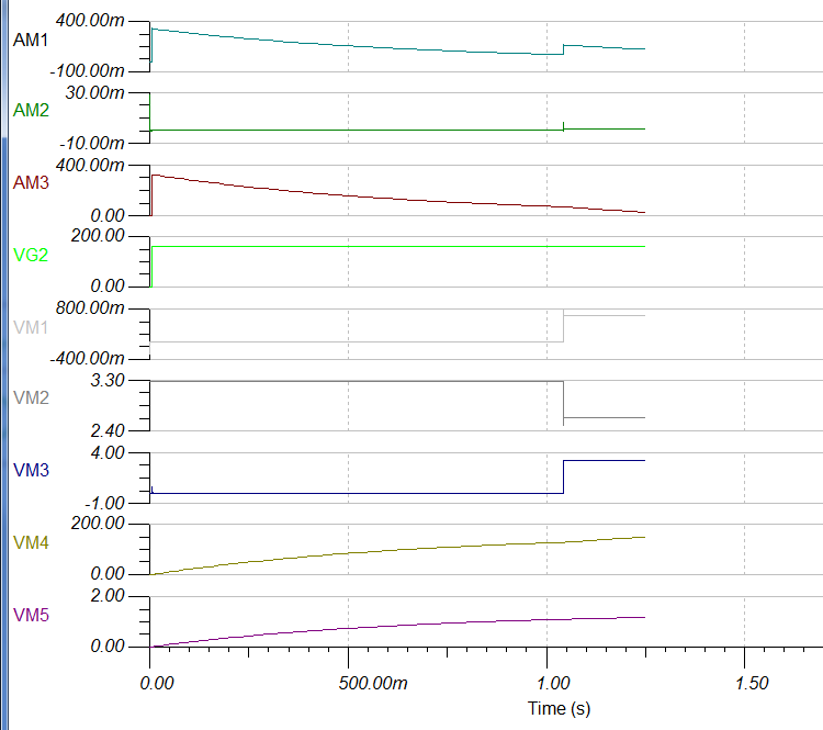
A similar more robust NFET circuit in Tina transient analysis shows very little inrush current vectors through DS in all transient modes, 470k resistive load tests. The ideal circuit uses an ICL (R4) across NFET and delays gate turn on for 1-1.5 seconds until C3,C4 caps are just above mid supply, ergo (90-163v). NFET directly replaces a bulky relay NO contacts bypass ground across ICL where the TPS output voltage slope control could perhaps remove the need for the ICL.

The ICL now remains reactive across on state NFET and ensures transient reverse currents from ground up to 40 amps are controlled. It doesn't seem plausible 40 amps or any current above a few capacitive ripple current amps or (dv/dt) would ever occur unless an HV caps suddenly shorts out. Transient analysis shows less than 700ma inrush current with 250/500 ohm resistor across the NFET DS when 163v is suddenly switched on.

Will dv/dt jotting below -0.3v destroy the TPS22969 NFET if the output (source) is tied to ground and the input (drain) faces the load? Secondly is there a Tina Macro available to simulate circuit operation?

Thanks for effort!

  • Hi BP101,

    Can you elaborate on what you mean by "Will dv/dt jotting below -0.3v destroy the TPS22969 NFET if the output (source) is tied to ground and the input (drain) faces the load?". This device does not have a dV/dt pin, but in general the -0.3V limitation is based on the ESD diodes on all of the pins. We do not recommend exceeding this limit.

    Also, you can request a TINA model in the simulation models forum.

    Thanks,

    Alek Kaknevicius

  • Hello AK,

    No dv/dt pin ??? dv/dt comes from an inverter FET switching noise or spikes appear at ground near T1. Had desired TPS22969 in place of T1 driven by T3. Later discovered Tina didn't graph VM4 was crossing supply voltage VG2 as a drop across R4 raising output voltage above device +5 BDV.

    Still is it possible for TPS22969 to drive NFET gate with added C to create an output voltage slope voltage rise at T1 gate?

    Load switch training video stated Webench can also do circuit designs around the TPS22969, is that true only for both +/- rails?

    Thanks for rapid reply!
  • BTW there is no Tina simulations forum in the forum list on left of search, even under development tools.
  • Hi BP101,

    Thank you for clarifying. The TPS22969 can be used to replace the load switching capabilities of the T1+T3. The TPS22969 already has a controlled output voltage slew rate, as specified in the datasheet. Do you need an adjustable slew rate for your applications? If so, devices like the TPS22975 and TPS22990 have a CT pin that can adjust the output slew rate through an external capacitance.

    The TPS22969 does not support negative voltages from input to output, and we do not have any load switches that can. Also, you can access the WEBENCH tool for the TPS22969 from the product folder.

    Thanks,

    Alek Kaknevicius

  • Hi AK,

    Tina later discovered the voltage rises at ground pins C3,C4 to 163v when NFET gate is off.  Though it wouldn't matter it seems that occurs any time a HV cap is not connected to ground the potential at one end equals the same at the other end, according to Tina results.

    Unless the output of the TPS229696 can withstand up to 200v it might simply blow up. I like the CT pin and was the reason for looking at this device to switch low side ground in the first place.

    Thanks for quick answers!