This thread has been locked.

If you have a related question, please click the "Ask a related question" button in the top right corner. The newly created question will be automatically linked to this question.

BQ76920: Highly inaccurate ADC reading

Part Number: BQ76920

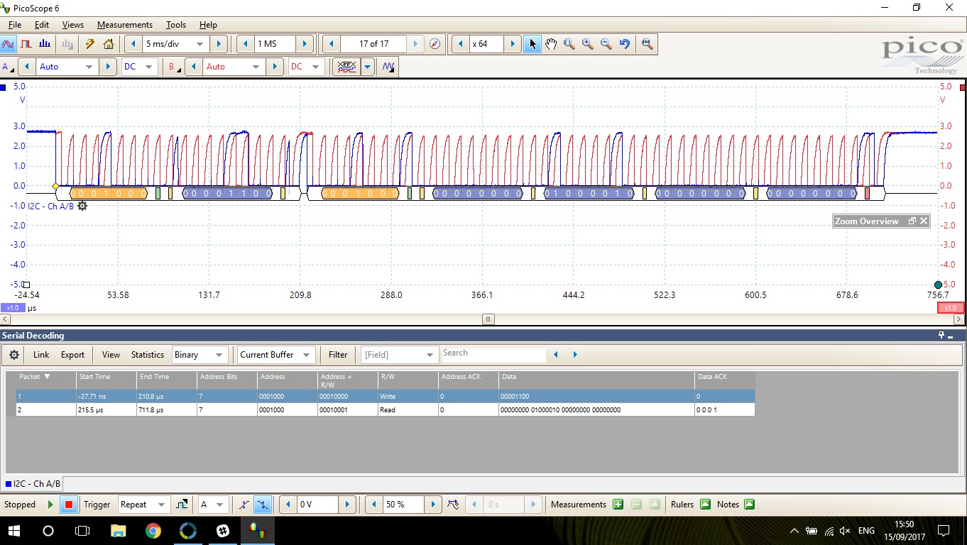
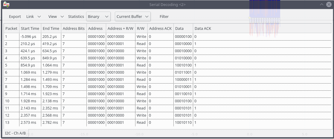
Thanks to previous help from this forum I have managed to establish I2C communication with the BQ76920. I am now trying to measure the voltage of Cell 5 using the internal ADC. Below is a screenshot of the I2C communication with the device.

  1. Select SYS_CTRL1 Register
  2. Receive SYS_CTRL1 Register
  3. Send modified SYS_CTRL1 Register back with ADC_EN bit set
  4. Select ADCGAINHI register
  5. Read ADCGAINHI register
  6. Select ADCGAINLO register
  7. Read ADCGAINLO register
  8. Select ADCOFFSET register
  9. Receive ADCOFFSET  register
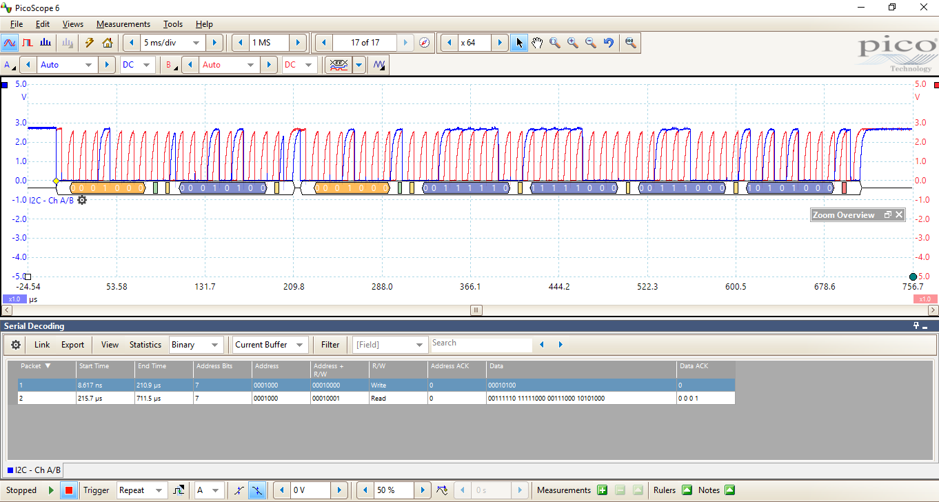
  10. Select VC5_HI register
  11. Read VC5_HI register
  12. Select VC5_LO register
  13. Receive VC5_LO register

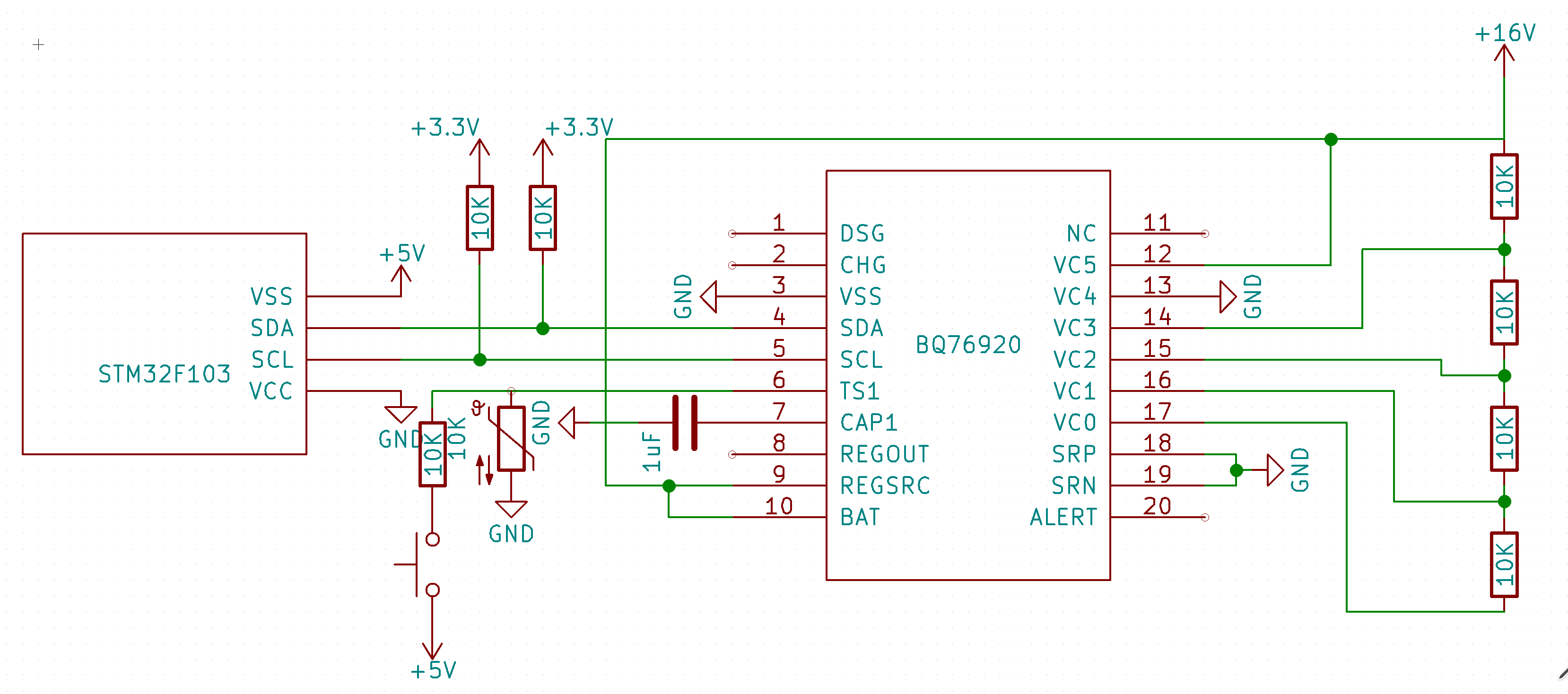
Analysing this data, ADC gain is 377 uV/LSB and offset is 50mV. The ADC value I read is 5526. Using the calculation Cell voltage = ADC*Gain + Offset, The voltage is 2.13V. The actual voltage is around 2.8V so this is quite inaccurate. The circuit used is shown below.

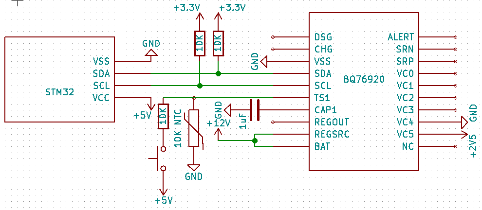
The Voltage on pin VC5 should read 2.8V. I will also include a link to an Imgur album containing traces of the LA here: https://imgur.com/a/lN7xt 

So my question is why is the ADC so inaccurate? Is my configuration of the Registers incorrect? Or is my circuit not complex enough?. Thanks for the help.

  • Hi Tom,
    The register read description shows individual byte reads. The register values for a voltage should be read sequentially with the same transaction to get an atomic value, note 7.3.1.1 and 7.5.2 in the data sheet. If the cell voltage ADC value is varying around 0x26FF and 0x2700, a separate byte read which crosses the time boundary of the value update could show 0x2600 or 0x27FF, an approximate 200 mV range. This is a common error source at certain voltages in an otherwise apparently OK system, but it is not likely your issue at the voltage stated.
    Your schematic is simplified, but shows only cell 5 connected with VC4 at GND. While not specifically stated, the device is not a collection of general purpose ADCs, it is intended for voltage measurement operation with a minimum of 3 cells connected in series with VC5 being approximately the same voltage as BAT. See Figure 8-1 and table 8-1 in the data sheet. The inputs must be operated with sufficient common mode to operate properly. You may have better results if you connect VC5 to the 12V BAT supply with VC4 2.8V below it, or if you apply your single ground-referenced supply at VC1 with respect to VC0, but it would be best to operate the part as intended with input filters similar to figure 8-1 in the data sheet. Resistors can be used to divide the supply voltage to simulate cells as is done on the EVM schematic if power supplies are limited. The part may be happy if REGSRC is 12V, but BAT should approximately follow VC5 (the sum of the cell voltages).
  • I have implemented the Battery simulation like you suggested, with battery being 16V and each cell being 4V. So  I shorted VC4 to ground. I am now having the problem where every register apart from VC5 is empty. Here is a picture of the I2C communication

    Here I am trying to read from VC1. Bytes 2 and 4 are CRC bytes. Why are the data bytes empty. Please help

  •  For more information I have included what the working register reads back. The cell is 4V, but using the calculation in the datasheet with the ADC value read from the registers, it is around 6.2V which is way out. So why is it inaccurate, and why is VC5 the only cell with data?

  •  I will also include the new schematic

  • Hi Tom,
    VC4 must not be grounded. See table 8-1 in the data sheet. By grounding VC4 you are shorting out the bottom 3 10k resistors through the balance FET internal between VC4 to VC3. This will put effectively 0V on the lower 3 cells, a negative voltage on cell 4 which violates abs max and probably about 15V on cell 5 which violates its abs max. The cell 5 ADC reads full scale.
    Remove VC4 from GND and connect it to VC3, connect VC0 to GND, then check your results. Connecting through filters would be better. There may be a resistive short internally across cell 5 now which will show as an unexpected low voltage on that cell. You may not want to trust this overstressed device.
  • On further thought cell 5 will see the full 16V rather than 15V mentioned above.
  • Thank you, I miss understood short as short to ground. I can now read from the other registers, but voltage is still inaccurate, about 2.4V instead of 4V.
  • Hi Tom,
    The part may have been damaged from the wrong connection. Without the filter components the values read from the device should be approximately what you measure across the 10k cell simulation resistors. If there is resistive damage to cell 5 pins it will decrease the top resistor voltage and increase the lower ones. If the ADC inputs are not damaged the sum of the 4 values should be the applied voltage (if all ADCs are in range). I'm glad you were able to make progress, it is probably time to replace the IC.
  • Ok, I will try with another IC and let you know what happens.
  • I have now tried with a separate IC. Initially testing was good, with VC5 and VC3 being accurate. I assume that VC4 is supposed to be 0V due to the short. However VC2, is inaccurate around 6.08V (should be 4V) and VC1 gives 0V which is incorrect. Is this a hardware issue?
  • Hi Tom,
    Glad to hear the voltages are correct on some. The voltage on the cell pins and reported by the part should be about the same as the cell simulation resistors. The 6.08V "cell 2" sounds like the ADC is at maximum, and the 0V "cell 1" sounds like the inputs are shorted together (as you measure and expected on "cell 4"). Check for a solder bridge between VC0 and VC1 or other unexpected VC1 to GND connection.
  • Everything working now with a new IC. Thanks for the help.