


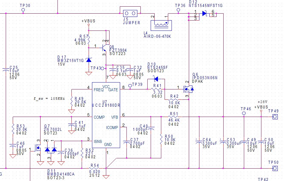
Schematic is shown below. Input voltage comes from rectified 12VAC, Vout = 28VDC, Pout = 70Wmax.
Everything works but I just noticed that Gate pin is ringing badly. What could cause this?
Thank,
Q6 GATE

U7 - PIN8

Q6 DRAIN

Schematic is shown below. Input voltage comes from rectified 12VAC, Vout = 28VDC, Pout = 70Wmax.
Everything works but I just noticed that Gate pin is ringing badly. What could cause this?
Thank,
Q6 GATE
U7 - PIN8
Q6 DRAIN


