Hello,
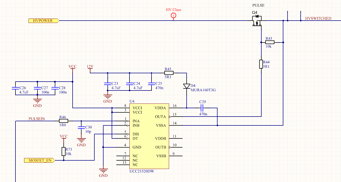
I have a design where one of my prototypes seem to have suffered a failure mode where the VDDA/VSSA pin (i.e., the output power pins 16/14) short together. I have attached a short schematic shot of the relevant portion.
The power MOSFET itself still seems to work, although I haven't yet verified there isn't some partial breakdown of it. Replacing the UCC21520DW on the board result in it working for a short time before this failure mode happened again. The failure mode passes significant current, as it results in R45 in the schematic burning up (the VSSA pin on the drain of the MOSFET connects to an inductive load, so when VSSA/VDDA shorts it means significant current passes through R45 since the inductive load is roughly a DC short to ground).
Once the short happens a low resistance (<2ohm) is measured between those two pins, even once removed from the board.
This happened on a later prototype, as an earlier one did not suffer this failure after extensive use. I'm still working on capturing all relevant waveforms but wanted to see if there was any suggested causes (i.e., exceeding dv/dt limits, catch diodes aren't fast enough on suppressing kickback etc). There was nothing obviously out of line from the captured waveforms but I need to confirm with some more in-depth tests.
If it seemed worthwhile I could have the devices sent to a FA lab, but I wasn't sure if the specific failure mode would have an obvious cause to the designers.
Some general design notes:
* HV being switched varies from ~200-500V. These failures were occurring around 300V.
* Only one channels is in use.