This thread has been locked.

If you have a related question, please click the "Ask a related question" button in the top right corner. The newly created question will be automatically linked to this question.

TPS659037: Power supply input sequence of TPS659037

Part Number: TPS659037

Hi,

5 V power of LDOUSB_ 1, 2 and LDO 12 _IN of PMIC rise first, then after 5 ms, VCC1 of PMIC and other 3.3 V power rise.
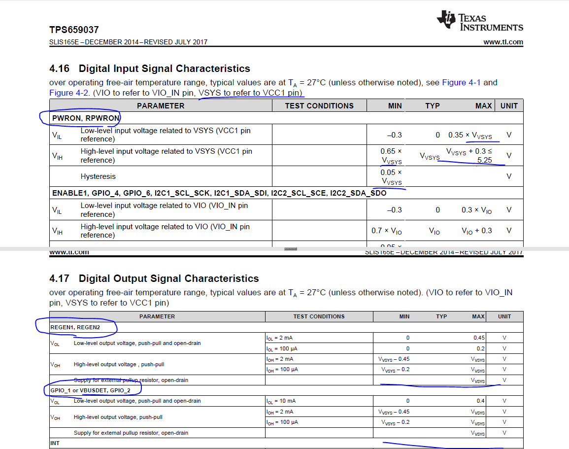
On the datasheet, in particular, I could not find the sequence regulation of input power of PMIC.
Is there any problem?

Best Regards,
Shigehiro Tsuda

  • Hi Shigehiro,

    I don't expect any issues with this order of power up. Part will not start sequencing until VCC1 power is valid.

    Regards,
    Jay
  • Hi Jay,

    Thank you for quick reply.

    I understood that the sequence does not start until the power supply of VCC1 is valid.
    Which is the best in the following two points?
    ①Supply VCC1 before any input power supply.
    ②Supply VCC1 after inputting another power supply.
    Since our customers are designing the circuit of power supply, please tell me the best way.

    Best Regards,
    Shigehiro Tsuda
  • Hello Tsuda-san,

    I do recommend supplying VCC1 first, before any other inputs. Section 5.3.1 of the datasheet describes this:
    www.ti.com/.../detailed-description

    The concern is, when VCC1 is unpowered, the power FET gate drivers are not working correctly, and for example there's no way to guarantee that the LDOUSB or LDO1/2 FETs are turned off. If the power FET is partially on, and there is voltage on the LDO input, it could get passed to the output. This could cause a glitch on the output which may not be wanted.

    If VCC1 is the same or greater as LDO inputs, this will not happen. We have observed this output glitch on LDOUSB when input is supplied before VCC1, and have not observed this behavior on LDO12. But I still suggest to power VCC1 before (or at the same time as) any other inputs.

    Regards,
    Karl
  • Hi Karl,

    Thank you for quick reply and the detailed explanation.

    Our customers are also satisfied with your answer and they are considering a circuit that supplies VCC1 at the beginning.

    Currently, our customers are considering a plan to enter 5 V instead of 3.3 V for VCC1.
    As a result of this change, is it correct with the recognition that the necessary PMIC terminal parts to be changed / examined on the circuit is the following?

    PWRON, RPWRON, REGEN1, REGEN2, GPIO_1 or VBUSDET, GPIO_2

    If there are other places that need additional consideration, please let me know.

    Best Regards,
    Shigehiro Tsuda

  • Hello Tsuda-san,

    Yes, those are the signals that will change. The VSYS inputs (PWRON, RPWRON, etc.) will need to be relative to 5V now, and the VSYS outputs (REGENx, etc.) will be 5V outputs.

    If you are changing any LDO inputs from 3.3V to 5V, then you'll also have to account for the increased power / heat through the LDOs. It is not required to change the LDO inputs, they can remain at 3.3V if your customer will still have this 3.3V supply.

    I don't expect any other impact to the PMIC.

    Regards,
    Karl
  • Hi Karl,

    Thank you for quick reply.
    It seems that our customers understood it according to your answer.

    It is an additional question.
    Is it correct when recognizing that VCC_SENSE and VCC_SENSE 2 should also be changed from 3.3V to 5V as described in the data sheet when VCC1 is changed from 3.3V to 5V?

    Please let me know if there is any change part by changing VCC_SENSE, VCC_SENSE 2 to 5V.
    The thresholds of VSYS_LO, VSYS_MON, VSYS_HI of the system voltage monitoring are exceeded, there is no limit on the upper limit so there is no problem recognition.

    Best Regards,
    Shigehiro Tsuda
  • Hello Tsuda-san,

    Yes, VCC_SENSEx pins should still be connected to VCC1. The thresholds of these pins stay the same, so the part still needs 3.1V minimum to turn on (VSYS_HI), and will shut off at 2.75V falling (VSYS_LO). I don't see any problem with this.

    Regards,
    Karl