This thread has been locked.

If you have a related question, please click the "Ask a related question" button in the top right corner. The newly created question will be automatically linked to this question.

WEBENCH® Tools/LM2676S-ADJEVM: LM2676 output ripple

Part Number: LM2676S-ADJEVM
Other Parts Discussed in Thread: LM2676

Tool/software: WEBENCH® Design Tools

Dear Sir, please, answer

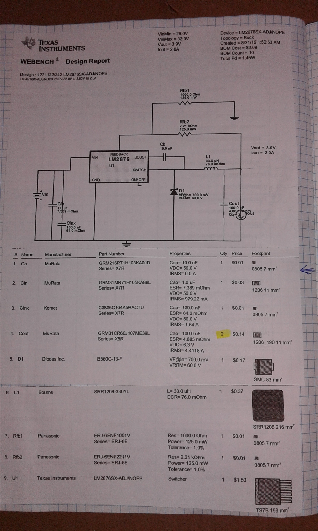
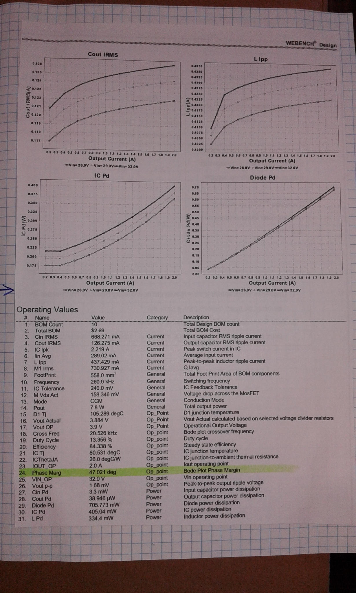
I use LM2676, please, see attach. Ripple on the out sometimes arises. And sometimes there is no ripple. I shot the oscillograms. If there is a ripple at the output, then the pulses at VD1_L4 are distorted at the front. If there are no ripple, then the pulses at the VD1_L4 are not distorted. L1 and L5 - are ferrite beards. PSB is two-layer.

L5 is now off. Output current  1.8- 2.0A - I connected external load.  If the out current is less than 1.7 A, then there is no ripple, but I need it to be 2 A.

I added two oscillograms of 'bad" ang "good" pulse on  VD1_L4. And and also, please, see the packed files

TIA

Sincerely

Vladimir NaumenkovLM2676SX.RAR

www.agat.by

  • Hi Vladimir ,

    Does the unstable switching happens only at higher load ?

    LM2676 is a voltage mode converter and the compensation needs to account for dual pole formed by output LC filter .

    I did some simulation on Webench and found that the electrolytic 820uF , 20mohm(6.3V caps like 6SVPC820M) capacitor at the output should be able to proplerly compensate the design . You should also be able to verify the compensation by going into the sim tab of the design .


    ----Ambreesh
  • Dear Ambreesh, thank you

    Yes it unstable at 1.8 A and more. But I need 2 A. 

    I do not use an electrolytic capacitor, because I need a temperature of minus 40 C

    Please, explain, why  my calculations in webench is wrong? Please, see below.

     Please, explain, what is it mean: "You should also be able to verify the compensation by going into the sim tab of the design."  ?

    TIA

    Sincerely

    Vladimir Naumenkov

    www.agat.by

  • Hi Vladimir ,

    What i meant was that you should be able to simulate the bode plot using the Webench .

    At our end , we will recreate the design and evaluate the same . You should expect the results soon .

    ---Ambreesh
  • Hi Vladimir ,

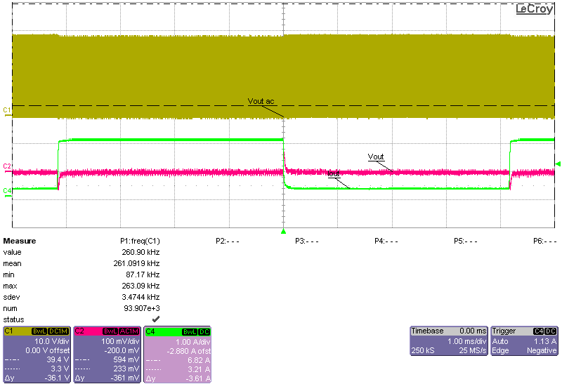
    We recreated  your design on our EVM and the design seems to perform well without any stability issue etc .

    In our evaluation with used same value inductor (with lower DCR which was available with us) as well as same output capacitors(2*100uF,6.3V,X5R).

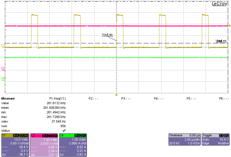
    Below are the waveforms -

    Output voltage and the Switch node (28V IN, 2A output )

    C1- Sw node C2- Output voltage C4- Iout 

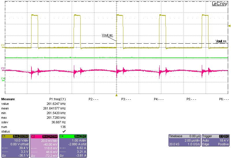
    Output ripple and Switch node 

    C1- Sw node C2- Output voltage(AC C4- Iout 

    Load transient to verify the Loop compensation and stability - 

    C1- Sw node C2- Output voltage(AC) C4- Iout 

    Here are few suggestions to move forward :

    1. Verify that the input power supply is not getting current limited .
    2. There seems to be no High frequency decoupling in your design .There seems to be multiple layout issues in your design. Either first evaluate your design on an EVM and use the EVM layout as an reference or try to rework your current PCB to make it better. 

    Let me know if you have any questions .

    ----Ambreesh 

  • Dear Ambreesh, thank you.

    Sincerely,

    Vladimir Naumenkov

    www.agat.by