Hello!
We need for technical support on BQ24171 device application. Our scheme is attached below; voltage levels are highlighted in red.
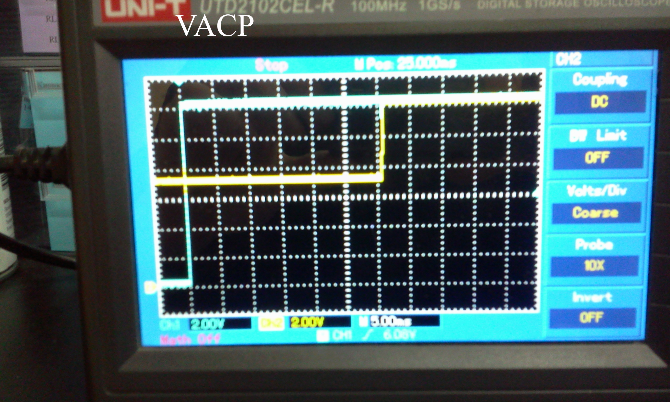
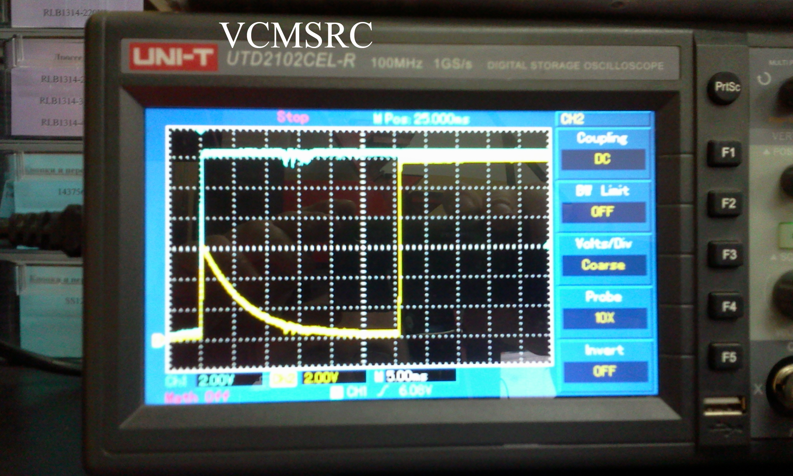
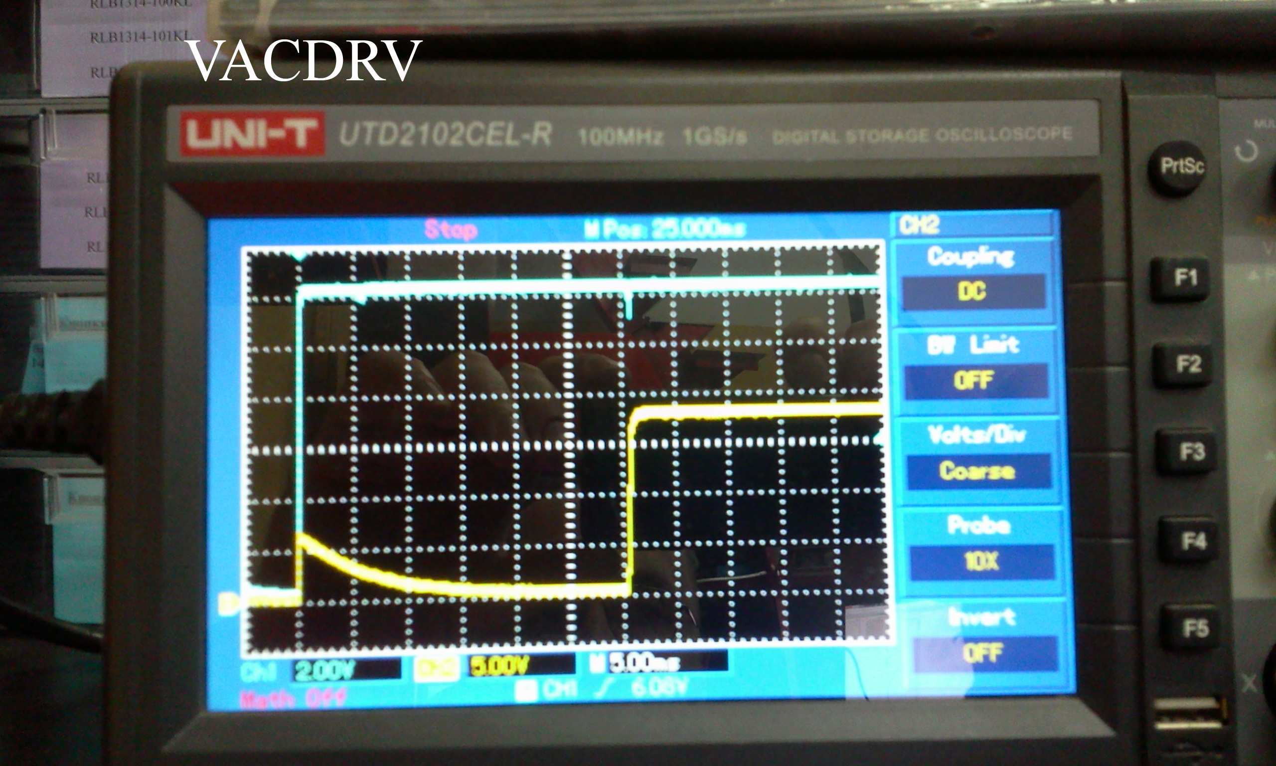
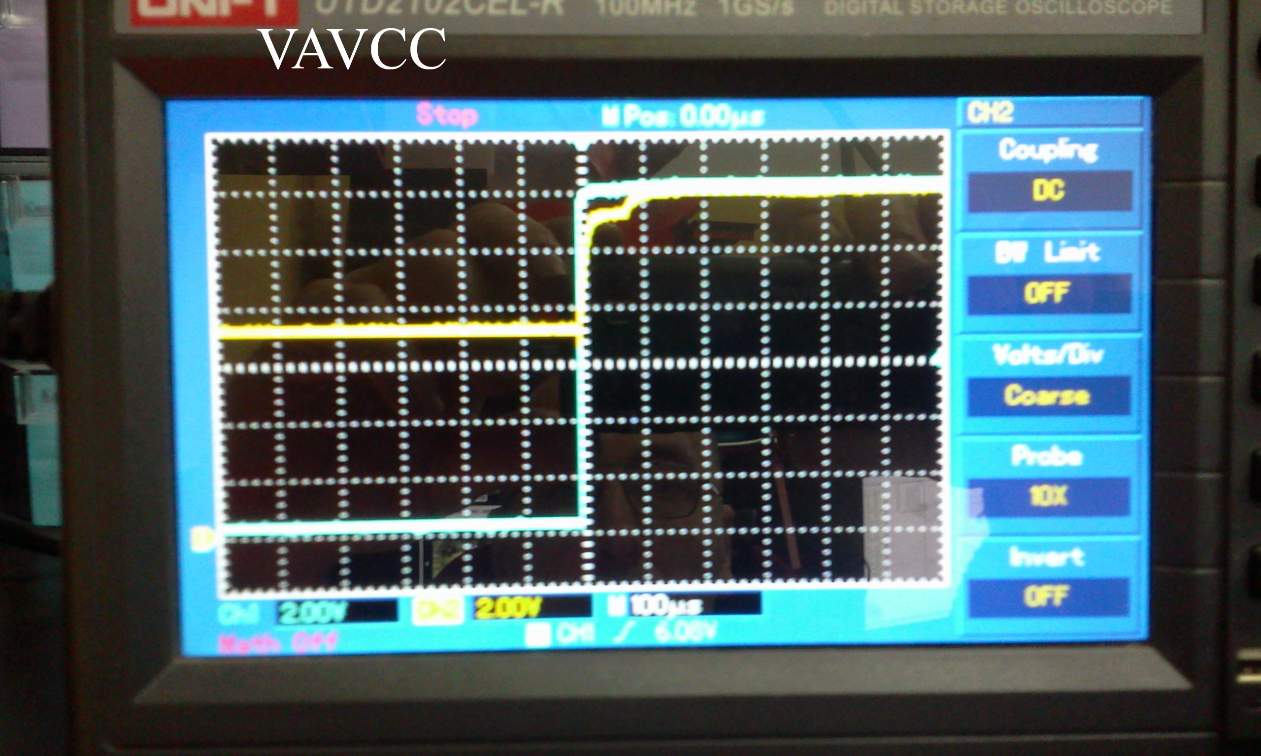
Scheme functioning doesn’t match the specifications, particularly paragraph 9.3.9 (Enable and Disable Charging). IC is in error state with 0.5 Hz output on STAT pin. As a result, IC doesn’t charge our cells. There is no any activity on SW pin.
We need to know:
- Are there any reasons for BQ24171 to be in error state except for the ones mentioned in 9.3.9?
- What can we do to find out why BQ24171 is in error state?