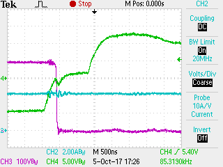
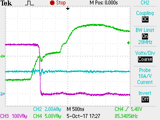
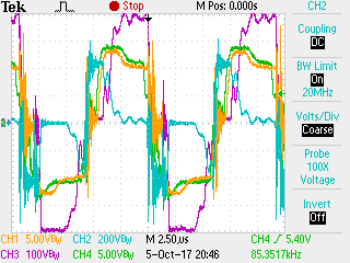
I am using an application with Vout = 150V Pout = 800W, Vin = 380V.
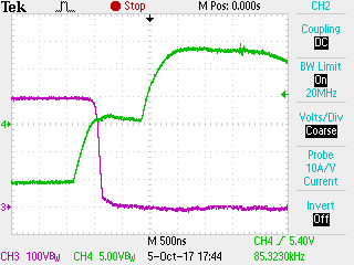
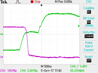
I see that Qa and Qb need higher output current to reach ZVS, around 2.0-3.8A output but Qc and Qd would reach ZVS at lower output current of 0.1 - 0.4A (100uH).
Qa = 3.8A
Qb = 2.0A
Qc = 0.4A
Qd = 0.1A
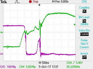
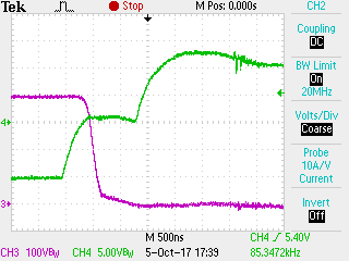
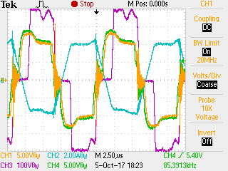
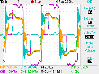
I also used 50uH.
Qa = 6.9A
Qb = 3.6A
Qc = 0.1A
Qd = 0.1A
Do you experience this and how to solve this?