This thread has been locked.

If you have a related question, please click the "Ask a related question" button in the top right corner. The newly created question will be automatically linked to this question.

LM3481: Hardware Technical Support

Part Number: LM3481

Hi Team,

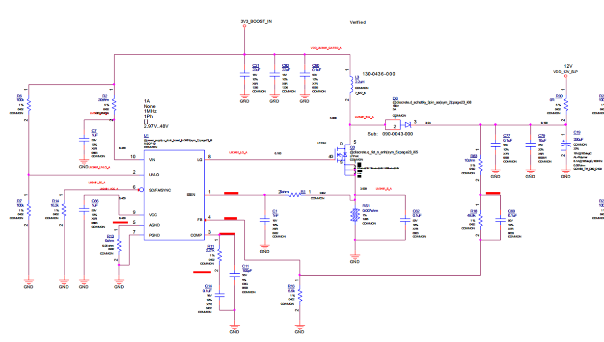
I have designed 3.3V to 12V Boost converter  circuit using LM3481 chip.But when i tested the circuit , i am unable to load more than 400 mA output load.i connected 12V dc Fan as load.

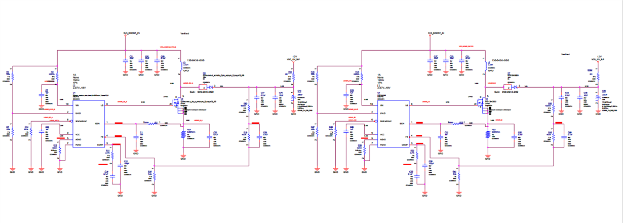
Here i attached the Schematic Design that i have. Please help me to rectify this issue. I used two stages for getting more output current.

  • It seems you set the circuit to run at 1MHz, and the converter may not have adequate duty cycle at that high frequency because of off timer inside. You can reduce your switching frequency to get higher load capability. Please use TI online design software Webench to help you modify the design.

    Regarding your approach of using two converters to support higher load, you cannot simply put two converters together. One must be in master and the other in slave mode. The master handles the feedback control, and the slave just need to follow. You need to short the FB of the slave LM3481 to GND and connect the COMP to the master's COMP. Then the outputs of the two converters can be tied together to share the total load.

    It's better to synchronize the switching between the two converters. Please refer to the datasheet.

    Thanks