This thread has been locked.

If you have a related question, please click the "Ask a related question" button in the top right corner. The newly created question will be automatically linked to this question.

Please explain datasheet [IGPK+ HI=LI=5 V, HO=LO=0 V, for PW <10us = 4A Typ.]

Guru 55913 points
Part Number: UCC27714
Other Parts Discussed in Thread: TIDA-00778

Finding the datasheet is not so clear in describing IGPK+ for conditions of 3v3 GPIO driving HI/LI and what is less than 10us PW relatively mean?

And 100ns = 10Mhz PWM frequency as described AMR Iout [Output current, HO, LO, IOUT_PULSED (100 ns) +/- 4A ]

If <10us PW = <100kHz can the IGPK+ 4 amps be produced with say a 50-80us HO/LO Ton PW driven by 12.5kHz to 20kHz PWM period?

Using the less than symbol to describe IGPK+ might be taken to mean a shorter PW as in nanoseconds or might even infer PW under 100kHz relative to the PWM frequency of the HI/LI inputs.   For example a 10us PW would not be considered less then a 10ns PW and much shorter or (<) 10us PW yet produces a much faster or (>) frequency. Seemingly the IGPK+ modulated PWM test conditions need to be disclosed in DS in order that IGPK+ of <10us PW has any relative meaning to HI/LI input of PWM frequency. 

Does IGPK+ PW <10us period infer 1us, 5us, .5us or perhaps 11us up to 100ns relative to HI/LI driving PWM frequency?

  • Thanks for your interest in TI here. I've contacted the appropriate product group. You should hear from them soon.
  • Hello,

    I am an applications engineer with TI and will work to answer your questions.

    For the question regarding the HI/LI input signal amplitude, as long as the input thresholds VINH and VINL are met, the signal amplitude does not affect the driver output current capability. The maximum input high threshold is 2.7V so 3.3V logic should be compatible.

    For the output current A Vs time conditions: When driving a MOSFET or IGBT which are capacitive loads, the driver is only sourcing or sinking significant current during the VGS rising and falling times. The high driver current is not required for the entire switching on time period. The ability of the UCC27714 to operate at lower switching frequencies, or longer pulse widths does not require the driver to source peak current for the duration of the on time.

    The <10us time mentioned in the datasheet is a test condition limitation for measuring driver output peak current into a short circuit, in a non repetitive condition. This is referring to the test condition for this parameter.

    Regards,

    Richard Herring 

  • Hi Richard,

    Richard Herring said:
    The <10us time mentioned in the datasheet is a test condition limitation for measuring driver output peak current into a short circuit, in a non repetitive condition. This is referring to the test condition for this parameter

    That's interesting as I have for the last 4 years believed vendors explanation of short circuit test indicated repetitive 10us pulses, not simply 1 cycle.

    Richard Herring said:
    the driver is only sourcing or sinking significant current during the VGS rising and falling times. The high driver current is not required for the entire switching on time period.

    I would challenge that notion based on text from IRF that suggests NFET DS current avalanche is a protective medium against device destruction and at the very same time can have premature avalanche from improper gate drive current. Seemingly we want the DS current to sustain somewhat relative to Ton period of the gate. Yet TIDA-00778 TI scope captures (fig.33-35) gate drive current indicates gate current falls in less than 250ns @15kHz and then fails to capture the DS current period relative to 80% gate drive duty cycle. So it seems the 250ns gate drive current is far to short to produce any real DS current and the IGBT is not entering forward Transconductance, EC saturation. May not be the case with an NFET under the same conditions but how would I know that by this TIDA publication?

    Hence the question how can IGPK+ <10us relate to the HO/LO Totem pole drive capability in actual device conditions with PWM driving HI/LI and AMR Iout pulsed 100ns/10Mhz Max be relative to actual device function in real time PWM conditions at a lower frequency, what is the Minimum Maximum PW? That might help to fill in the void of information.

    The data sheet fails to address actual working conditions of the UCC relative to low frequency PWM input conditions (8-20kHz) and seemingly focuses on high frequency conditions in the AMR.

  • BP101 said:
    I would challenge that notion based on text from IRF that suggests NFET DS current avalanche is a protective medium against device destruction and at the very same time can have premature avalanche from improper gate drive current.

    That is speaking relative to an (unclamped) inductive load being driven by the UCC gate driver.

  • BP101,

    I am an applications engineer who works with Richard. I will be responding to future questions in this thread.

    BP101 said:

    I would challenge that notion based on text from Infineon that suggests NFET DS current avalanche is a protective medium against device destruction and at the very same time can have premature avalanche from improper gate drive current.

    Can you please provide a link to this text?

    BP101 said:

    Hence the question how can IGBPK+ <10us relate to the HO/LO Totem pole drive capability in actual device conditions with PWM driving HI/LI and AMR Iout pulsed 100ns/10Mhz Max be relative to actual device function in real time PWM conditions at a lower frequency, what is the Minimum PW? That might help to fill in the void of information.

    AMR Iout pulsed should be taken as a limit on the pulse current, not on the pulse duration. 4A for 200ns does not violate AMR, but 4.1A for any duration does violate AMR.

    IGPK is specified because discharging a fully charged gate capacitance to ground, or charging a fully discharged gate capacitance to VDD/HB, can behave similarly to a temporary short circuit on the output. With typical conditions, a short circuit (or similar behavior) on the output lasting <10µs should cause an output current of 4A typical.

    The AMR Iout pulsed rating and IGPK do not, by themselves, limit the frequency. The minimum PW is 100ns worst case for both high and low input pulses, theoretically limiting the maximum achievable frequency to 10MHz.

    I recommend taking a look at the application note Fundamentals of MOSFET and IGBT Gate Driver Circuits, specifically sections 2.5 and 2.6.

    Regards,

  • Hi Derik,

    Derek Payne said:
    The minimum PW is 100ns worst case for both high and low input pulses, theoretically limiting the maximum achievable frequency to 10MHz.

    Again what is the maximum PW if that is the AMR maximum frequency (10Mhz) @100ns Min PW relative to output section of DS IGPK+/-?  Seemingly that AMR 100ns does not express the maximum PW by indicating IGPK+/- @<10us and is not taken by designer as a single cycle pulse test. The output section DS should express IGPK+/- PW of 1us will work equally as well as 80us PW if HO/LO are not shorted to ground since there are no BW graphs. Seemingly the DS output section and AMR fails to explain IGPK+/- when a 35us pulse train is driving HI/LI as to what the expected IGPK+/- amps can it produce. There are no graphs to indicate HO/LO IGPK+/- at any relative PWM frequency. The UCC is a PWM NFET gate driver and should have several IGPK+ /- current related graphs relative to the input frequency BANDWIDTH of the HI/LI inputs. 

    You have not truly answered any of the questions asked relative to IGPK+/- peak <10us being listed under EC section of DS and contradicted by Richard as being a single cycle test measure.  How else can anyone know what the HO/LO output structure can source/sink relative to Ton of the NFET if it is not properly documented relative to HI/LI PWM frequency in graph plots? Point is we can't and have to take the DS 4 amp claim at face value and pray to the gods it don't smoke if the IGPK+/-  PW rises well above 10us.

    So far I have not seen any evidence that UC27714 can actually source or even sink 4 amps in a duration other than AMR with PW 100ns which is not the recommended operating conditions. There is no documented IOut range relative to input frequency being described in DS so the design engineer can relate PW and PWM (duty cycle %) to HO/LO current drive. Again is the IGPK+/- <10us a 50% PWM duty cycle repetitive short to ground or single cycle test? If single cycle how can that be considered the only evidence for HO/LO IOut +/- 4 amps especially in the recommended operating conditions. Point is it can't  give the designer any useful information other than a single IGPK pulse to ground above 4 amps PW perhaps >10us will destroy the HO/LO output structure.

    Derek Payne said:
    I recommend taking a look at the application note 

    That is not the point of this post as to point out to TI engineering the lack of important data graphs or other means to express IGPK+/- 4 amps being claimed in AMR and EC sections of DS express mostly conjecture. Conjecture is hypothetical information with no actual proof or evidence to back it up when it is called into question. 

    All NFET have current avalanche under conditions of unclamped inductive kickback on the wire or from other active switch nodes on the same (shared) wire, such as 3 phase commutation. Seemingly if (IGPK) is not kept constant during the miller plateau the parallel tunnels will collapse (avalanche) or perhaps even the parasitic BJT could trip if the GS voltage rises should gate current suddenly drop (<10us) under very heavy IDS. So 250ns IGPK+ may seem like a lot of time but in light of inductive kickback it my take a much longer IGPK period to maintain high IDS under EMF conditions. Good reasons for having graphs to indicate gate drive IGBP at specific frequency curve in the BW relative to temperature. 

    I^R AN1005 page 4-17

  • Richard Herring said:
    The <10us time mentioned in the datasheet is a test condition limitation for measuring driver output peak current into a short circuit, in a non repetitive condition. This is referring to the test condition for this parameter.

    Please review the DS output block [IGPK+/- <10us] HO/LO high/low (pulsed current short circuit to ground). That test result infers logically when HO/LO is not shorted to ground the current is relative to inline HO/LO series resistance, PU=3.75-5.8 ohms PD=1.45 ohms. Any added gate resistance will change the pulsed current short circuit results and a higher PW >10us say even 35us Ton will produce a different IGPK+/- current other than 4 amps. I don't care about the IGPK peak so much rather the results at various input frequency in the 10Mhz BW would be more important to more effectively control the NFET Miller plateau region.

    Therefore a DS curve graph is required to show the UCC does not produce 4 amps at lower HI/LI input frequencies below 100kHz.... Just because everyone in the industry does it this way is no excuse.

  • Derek Payne said:
    I recommend taking a look at the application note Fundamentals of MOSFET and IGBT Gate Driver Circuits

    The page no longer exists.

    Recommend TI update TIDA-00778 and capturing the IGBT high voltage trapezoidal output wave form, not just showing the UCC27714 gate drive signals. Would be helpful to see the actual results of the intended DSP using UCC27714 to produce a better output wave shape, perhaps with less undesired current avalanche.

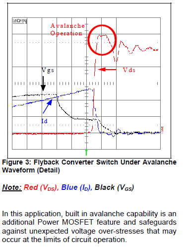
    That unclamped current avalanche occurs most pulses (source 350ma/sink 650ma) and not result of body diode (dv/dt) as some FE suggest as switch node noise ringing shown in the red circle AN-1005 page 4-17.

  • Hi DK,

    I edit typo IGBP in all posts and meant to suggest Maximum PW for IGPK+/- >10us in post with your response of AMR frequency 10mHz(100ns). Current avalanche seemingly an undesired product of NFET but occurs in solenoid drive circuits and apparently in 3 phase motor commutation. I have recently become aware that is not so good if it cycles yet IAs is typically shown in NFET DS as an energy product but seems to also result in reduced DC inverter efficiency.

    Seemingly the low frequency PWM and even high frequency PWM in the best of circuit designs can produce IAs, when less of it is better. The idea it seems to arrest IAs is to hold the Miller plateau from collapse when outside wire (EMF) is attacking from all sides. That's my take on what is happening cause our current vendors gate driver.
  • BP101,

    Thank you for pointing out the broken link, I have updated it in the original post. The link can also be found here.

    I agree with you that including the switch node waveform, as well as perhaps the current waveform, would be more conclusive evidence that the driver is functioning properly. I will convey this feedback to the design owner.

    BP101 said:

    That unclamped current avalanche occurs most pulses (source 350ma/sink 650ma) and not result of body diode (dv/dt) as some FE suggest as switch node noise ringing shown in the red circle AN-1005 page 4-17.

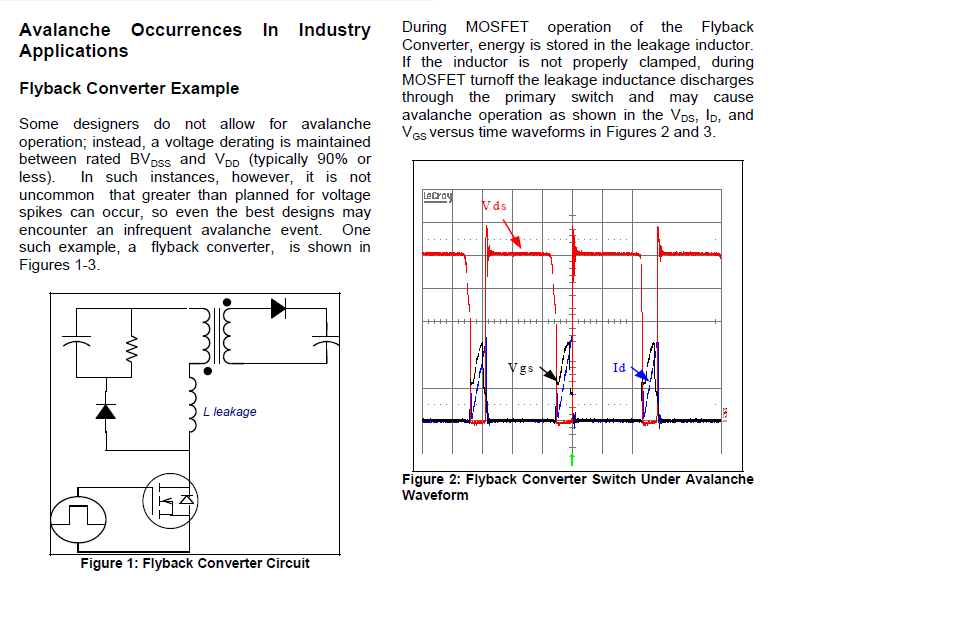
    I don't think I understand what you mean by an unclamped current avalanche. Avalanche breakdown occurs from drain to source due to overvoltage stress. The ringing overvoltage is a function of the inductance and the rate of change of current, so because the inductor current declines quickly during NFET turn-off in a flyback or with some other inductive load, this causes very high ringing which could cause avalanche breakdown to occur. Is this what you mean by unclamped current avalanche?

    I am still looking into IGPK rating. I will update you once I have more information. 

    Regards,

  • Derek Payne said:
    Avalanche breakdown occurs from drain to source due to overvoltage stress.

    Or perhaps the ringing in red circle is actually the aftermath of a PN junction collision with EMF in the unclamped inductive (UCI) load such as a solenoid would present to the NFET if the CCEMF is not snubbed. Even the best of circuit designs with a clamped inductive load experience occasional IAs.

    Derek Payne said:
    so because the inductor current declines quickly during NFET turn-off in a flyback or with some other inductive load

    That's my point the actual turnoff event or (perceived) fall in gate drive voltage is due to the IAs event near the end of each PWM period of another node on the wire, not the other way around. The ringing in the coil is the result of IAs as drain voltage suddenly snaps back to full VDD. It just so happens the EMF event in each IAs cycle coincides with the PWM period end and fakes everyone out. We don't clamp the load in 3 phase commutation so the EMF is always present and IAs occurs end of every most PWM cycles and drives down inverter efficiency as the NFET junction heats from excessive IAs events. The event occurs so fast test instruments can not detect the start of NFET DS gate field collapse until after the IAs event occurs. Seemingly we only see the remnant of the IAs collision and think that is normal switch behavior.

    Question is can IAs (avalanche) be arrested by holding gate current high during EMF of another active switch node. In the past 4 amp gate drivers never existed and we only see the old IAs behavior from very low gate current drive.


  • Hi Derek,

    Derek Payne said:
    I agree with you that including the switch node waveform, as well as perhaps the current waveform, would be more conclusive evidence that the driver is functioning properly. I will convey this feedback to the design owner

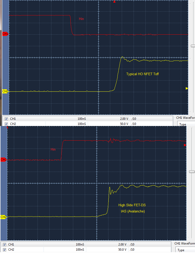
    That would be a huge gain to compare IGPK drive current of various gate drivers to the 4 amp IGPK of UCC27714. The IAS (avalanche) events are the concern as mentioned the event seems to occur randomly even with high speed Hex-FET having a 39 amp IAS specification.   

    Notice the top capture faked me out thinking it was the LO switch tuning off when in hind sight it seems the very same HO switch (bottom capture) but with an IAS avalanche event. Adding more HO/LO gate drive resistance did not help so much at higher BVDSS above 80v, rather helped more at low voltage 24v. Captures; Working voltage 162v-138v,  HO/LO 60/10 ohm, IGPK <10us short to ground, 350ma source / 650ma sink.....


  • Derek Payne said:
    I agree with you that including the switch node waveform, as well as perhaps the current waveform, would be more conclusive evidence that the driver is functioning properly. I will convey this feedback to the design owner

    Regarding my comment of the lack of data sheet graphs & plots; A curve showing PWM frequency 0-10Mhz bottom grid and IGPK+/- for HO/LO outputs on vertical grid but at various temperature values -40,25,150 degrees Celsius. Perhaps another graph showing IGPK+/- values of fixed PW produce an HO/LO drive current at various PWM frequency 0-10Mhz  (not simply claiming IGPK is 4 amps Max)  PW<10us shorted to ground. Obviously the AMR Output 4amp (100ns) indicates as you point out the maximum PW or frequency and leaves a void in proper disclosure.

    The problem with this datasheet and others like it is they do not express the HO/LO IGPK PW conditions above older 350ma/650ma gate drivers. What is to gain by us switching to a higher current gate driver? That seemingly is not being expressed in the datasheet other than it offers best in class propagation delays and better pull up control of Miller Plateau on HO output and a few other nice features. Point is the 4 amp claim being made seems to get lost in the disclosure. Not to forget adding a 5.1 ohm series resistor with VDD will produce a voltage drop at the VDD pin since the hold cap will never reflect the true measured voltage of any sourced VDD. This fact is mentioned in IR datasheet relative to Cboot peak charge falling below VDD due to Rboot voltage drop.