This thread has been locked.

If you have a related question, please click the "Ask a related question" button in the top right corner. The newly created question will be automatically linked to this question.

BQ76940: Do I need to connect Cell 0 and Discharge lead (BATT-) to GND ?

Part Number: BQ76940
Other Parts Discussed in Thread: TIDA-00255

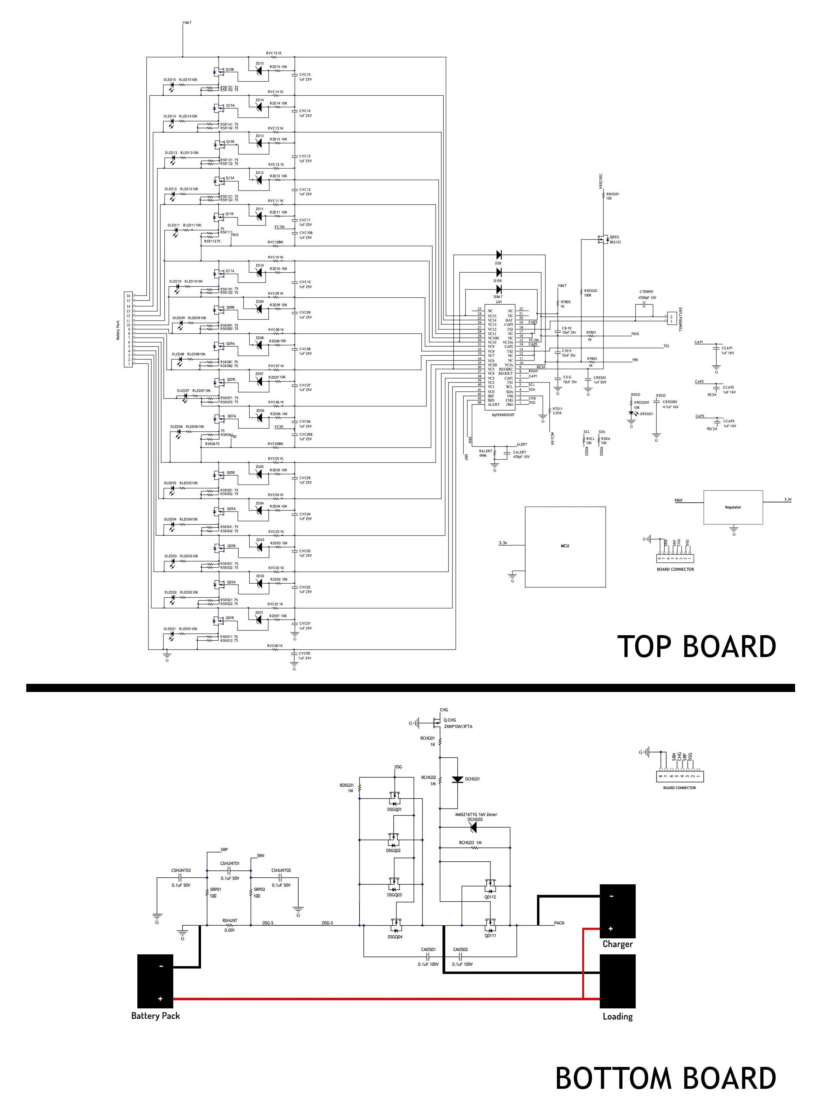
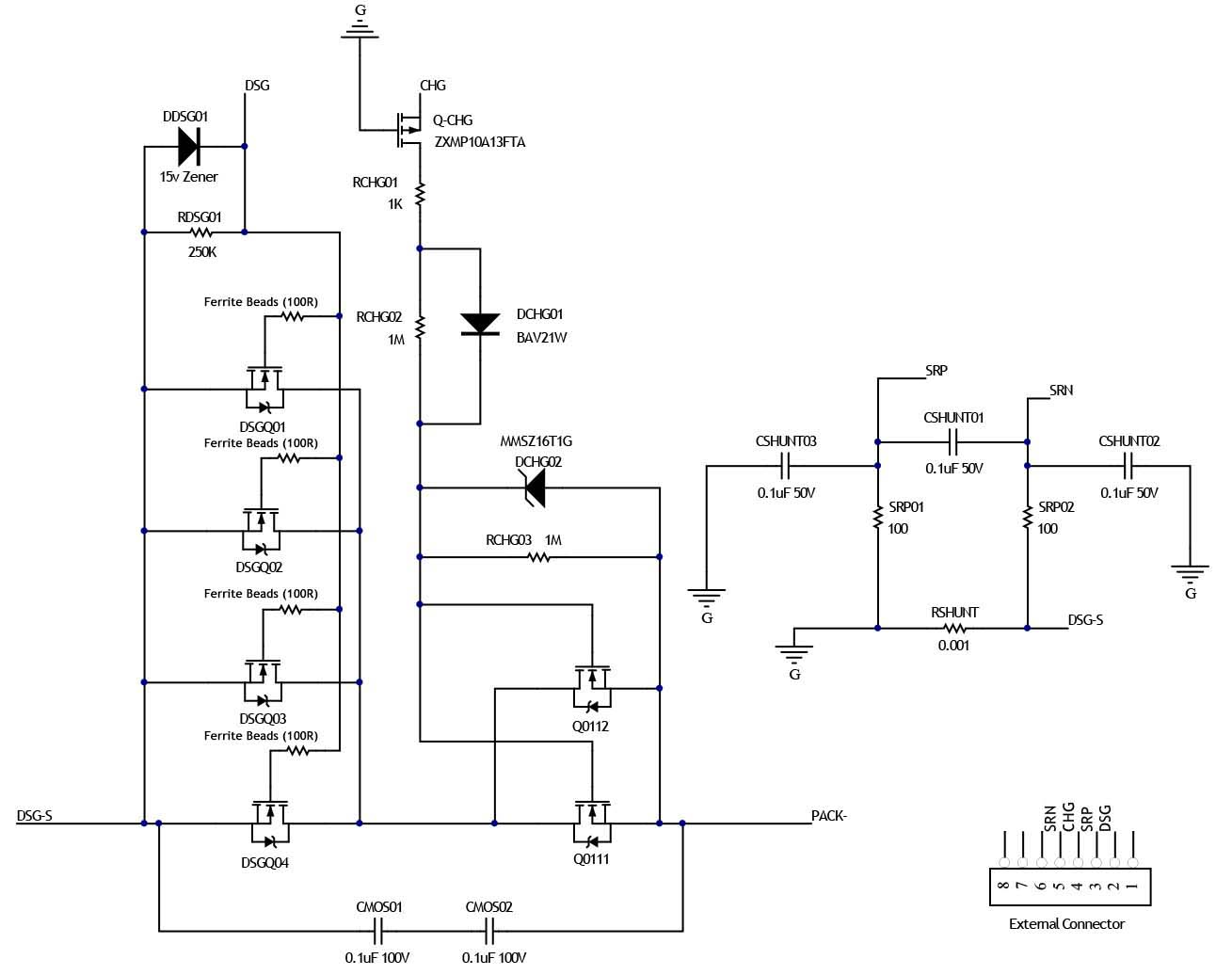
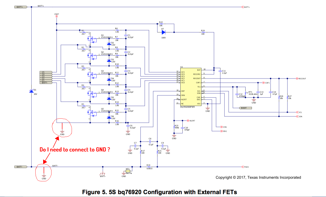
attached is schematic from SLUA810, the BATT- and Cell 0 are not connected to GND that's different from other TI suggested schematic, is that's any problem  ? 

  • Hi Tiger,
    Yes, you need to connect VSS of the IC and its related components which connect to GND to BATT-. In the schematic the upper connection you have shown is connected to GND by the net name BATT-. The lower connection of BATT- to GND is accomplished through the NT1 component, it is a way in this design tool to connect 2 nets through a controlled size copper connection. The size of the copper connnection is not critical, the situation to avoid is having the pack load current flowing between GND connections for the various filter or references for the electronics
  • Hi,

    thanks for your quick response, now i have huge trouble that all my 10 x demo board sent to our beta testers were damaged, all related to MOSFET with GATE and SOURCE shorted caused even 1A current loading, now i suspect it was grounding issues and caused over GATE voltage ?  

    attached my schematic, i have connect board GND together via board connector, TOP BOARD's GND connected to cell 0 or BATT- and board connector, BOTTOM BOARD's GND connected to board connector and BATT- (main discharge lead).

    TOP BOARD's powered by Cell 15 or VBAT connected to Voltage Regulator -> 3.3v -> MCU 

    BOTTOM BOARD BATT+ just by pass 

    Thanks in advance,

     Tiger

  • Hi Tiger,

    I don't immediately see a problem with the circuit.  The battery negative is connected to the Battery Pack connector negative and to ground on the bottom board, to the Battery Pack connector pin 1 of the top board, and also through the Board Connector pins 7 and 8.  There may be some current through the board connector back to the battery, but I would not expect this to damage the FETs.

    Adequate but not excessive gate voltage and sufficient switching speed are common concerns to avoid FET damage.  The CHG and DSG voltages are internally regulated in the bq76940 at approximately 12V, so this should not be a concern with FETs having a 20V max Vgs.  The supply is from REGSRC.  You might be sure QREG is able to provide continuous supply to the IC so that the gate voltage would not drop out.  REGOUT is also powered by REGSRC but at a much lower voltage.   RREG01 is supplied by the net VRECSRC, I did not recognize this point on the schematic, it normally comes from the top cell.  You might also check this connection.

    If the Board Connector came loose during operation the FETs would slowly turn off by the 1M resistor RDSG01 on the bottom board.  With 4 FETs this could be very slow and if load current is flowing the FETs could be overstressed.

    Check the FET temperature under system operation to be sure the temperature is within specifications.

    You might also look at the performance of the FETs when switching.  The bq76940 has the internal resistive driver.  More FETs will increase the load during switching and slow the switching speed causing heating.  Also check your FET manufacturers recommendations for parallel FETs.  Some FET experts recommend a small resistance to each gate compared to the common  resistance to avoid high frequency oscillation which can result in FET damage.  Some recommend ferrite beads for high frequency impedance with low DC resistance. The need for the resistance seems to depend on the FET design, we have used ferrite beads on several EVMs to suppress oscillation.

  • Hi,

    Thanks for your suggestion, I have changed few things according to your suggestions, could you please help again to review it ?

    1. each MOSFET gate added 100 ohm ferrite beads
    2. changed gate source resistor from 1M to 250K to reduce fall time
    3. add 15v zener diode to prevent over gate source voltage
    4. remove GROUND connect from top board to bottom board because it is not necessary

    However up to this moment, I still have some question regarding the TIDA00255 reference design.

    according to the altium Designer (TIDA-00255 Altium) document, the AFE top's C0 pin connected to Mosfet section (FETs.schdoc) which is BATT- via R1 (even on schematic which is marked DNP), and the Mosfet section BATT- has no direct connected to any GROUND point beside NT1 (however on reference board photos, which is left 2 holes without put on, perhaps it is optional component ?)

    now my question are :

    1. without insert NT1, look like nowhere that BATT- or C0 is connect to GROUND
    2. how's the NT1 function, resistance inverse proportional with temperature ?

    Thanks,

    Tiger

  • Hi Tiger,
    As assembled the EVM or TIDA-00255 has the bottom cell connection "C0" made through a wire to the cell separate from the high current wire. R1 would be an option to sense locally and avoid the C0 wire.
    1. Correct, NT1 connects the GND plane to the high current path BATT-. NT1 is placed from the library, but is constructed in etch on the board, it is a physical piece of copper left when the board is etched, it is not a installed component.
    2. NT1 is just copper trace. On the board it is a narrow.
  • Hi,

    Oh yes, I re-checked there's a narrow trace connect BATT- and GROUND, sorry about that.

    Also I have changed few things according to your suggestions last time, could you please help again to review it ? 

    1. each MOSFET gate added 100 ohm ferrite beads

    2. changed gate source resistor from 1M to 250K to reduce fall time

    3. add 15v zener diode to prevent over gate source voltage

    4. remove GROUND connect from top board to bottom board because it is not necessary

    Thanks,

    Tiger

  • Hi Tiger,

    The changes may be fine but you may want to check:

    1. MOSFET gates with 100 ohm ferrite beads, may be fine

    2. The DSG gate source resistor from 1M to 250K to reduce fall time: This may not make much difference in normal operatoin, will draw more current when on. If the connection between boards is lost it will turn off faster, you would have to test to see if it is fast enough.

    3. The 15v zener diode on DSG: Since the diode should never conduct and you want to avoid leakage, you might used the same diode as the CHG gate.

    4. Remove GROUND connect from top board to bottom board: If you have grounded the top board through the C0 sense connection you should not need the connection between boards.  But consider whether you may want the ground through the connector and use the C0 sense only for measurement & balancing rather than the IC ground reference.  When the boards can be separated consider if your system needs protection on the pins from transients, see the discussion in slua749 section 10 around figures 22 to 24.

  • 1. I have compare TIDA-00255 with Ground at Sense Resistor and Remote Cell Sense, Ground at Sense Resistor and Local Cell Sense and Ground at Remote Cell Sense 3 approaches and didn't find match with, or Ground at Sense Resistor and Remote Cell Sense approach without DVC0 zener right ?

    2. Now look like "Ground at Sense Resistor and Remote Cell Sense" approach not applicable because my upper board can work as standalone balancer that's need Ground on upper board.

    Can I take "Ground at Remote Cell Sense" approach but connect Sense circuit with ground from upper board via board connector ?

    3. then what is the zener value for sense circuit ?

    enclosed is my design (pink is upper board, and blue is bottom board) will take "Ground at Sense Resistor and Remote Cell Sense" with board connector provide GROUND to bottom sense circuit, please help to review it. 

    Thanks,

    Tiger

  • Hi Tiger,
    In the modified circuit above it may be best to have the limiting and filter for SRP & SRN with the IC since it is the IC which does the measurements and has the abs max restrictions. The connection to the bottom board is to sense the current and control the FETs. The bottom board does not need the filter to flow current.
    The zeners should be selected to avoid abs max of the pins, -0.3 to 3.6V max. You want to avoid leakage of the zeners from influencing the normal signal, so select a value which will protect the pins from the expected levels which could be applied in the system.
    It seems you have 2 systems on the same board. When operating only the top board you need a VSS connected at the the cell connector with protection on the SRN/SRP. When operating with the bottom board it seems you would want VSS referenced at the sense resistor for good current measurement and reference near the FET source then limit the signal range to VC0. You will know your system best and can determine what configuration or options you may need for the boards.
  • Sorry to bother you again, my last diagram was based on your suggestion to follows the "GROUND AT REMOTE CELL SENSE" approach because I think this approach closely match my design (standalone top board need GND or VSS reference, so connect to C0), however unlike Figure 24, my board is separated, the SENSE filter circuit is located on bottom board therefore I need GND or VSS reference, so I take GND or VSS from top board via board connector (you can see the RED line and BOARD CONNECTOR from my diagram).
    and the zener of on SENSE filter circuit is TI suggested because of REMOTE SENSE approach figure 24.

    Do you mean that I should / can locate the SENSE filter circuit to top board, then I don't need GND on bottom board anymore and 100% follows TI's figure 24 "GROUND AT REMOTE CELL SENSE" suggestion.

    Once again, thanks for your support, I already order PCB boards for this approach to see if damage MOSFET can be resolved which is based on your valuable parallel mosfet suggestions.


    Thanks,

    Tiger

  • Hi Tiger,
    Right, the IC sees the voltages relative to its VSS, so having the filter near the IC inputs (on the top board) is generally considered best. The signals will be filtered (and limited) relative to the VSS pin and should provide best protection, noise pickup or disturbances between the filter and the IC pins should be minimized. In this case there is not a need for a ground to the bottom board for the sense inputs since it is sensing differentially and the sense resistor has ground back to the cells. Two areas of concern might be:
    1. If the high current path from the sense resistor back to the cells has a high resistance/impedance, the clamp diodes may conduct and the sense voltage is influenced by the clamp currents.
    2. The DSG pin is referenced to the VSS of the IC, if the path from VSS to the cells through the sense path (B0 in figure 24) and back to the FET through the high current path (B- in figure 24) and sense resistor has a high impedance that may affect the discharge FET turn off. You might check this in your testing. If improvement is needed a capacitor between the GND of the upper board and the lower board may bypass the impedance of the wiring to the cell, or in some systems a driver is added with the FET so that the FET gate current has a shorter path.