This thread has been locked.

If you have a related question, please click the "Ask a related question" button in the top right corner. The newly created question will be automatically linked to this question.

UCC27211: Getting incredibly hot in synchronous buck converter application

Part Number: UCC27211

Hello,

See my circuit below,

I'm seeing high temperatures with minimal load on the mosfets (few watt's). When I turn up the load the mosfet driver keeps getting hotter and hotter until it gets too hot and shuts down.

I have seen case temperatures of 100 degrees Celsius +.

My application is as follows:

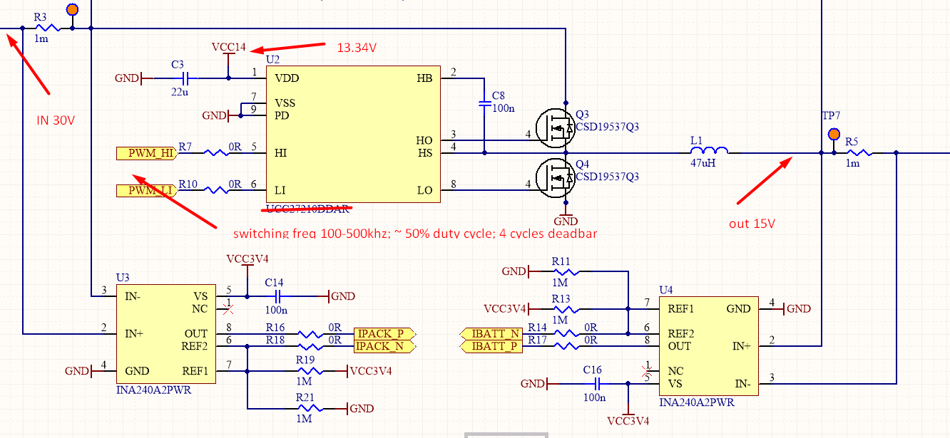
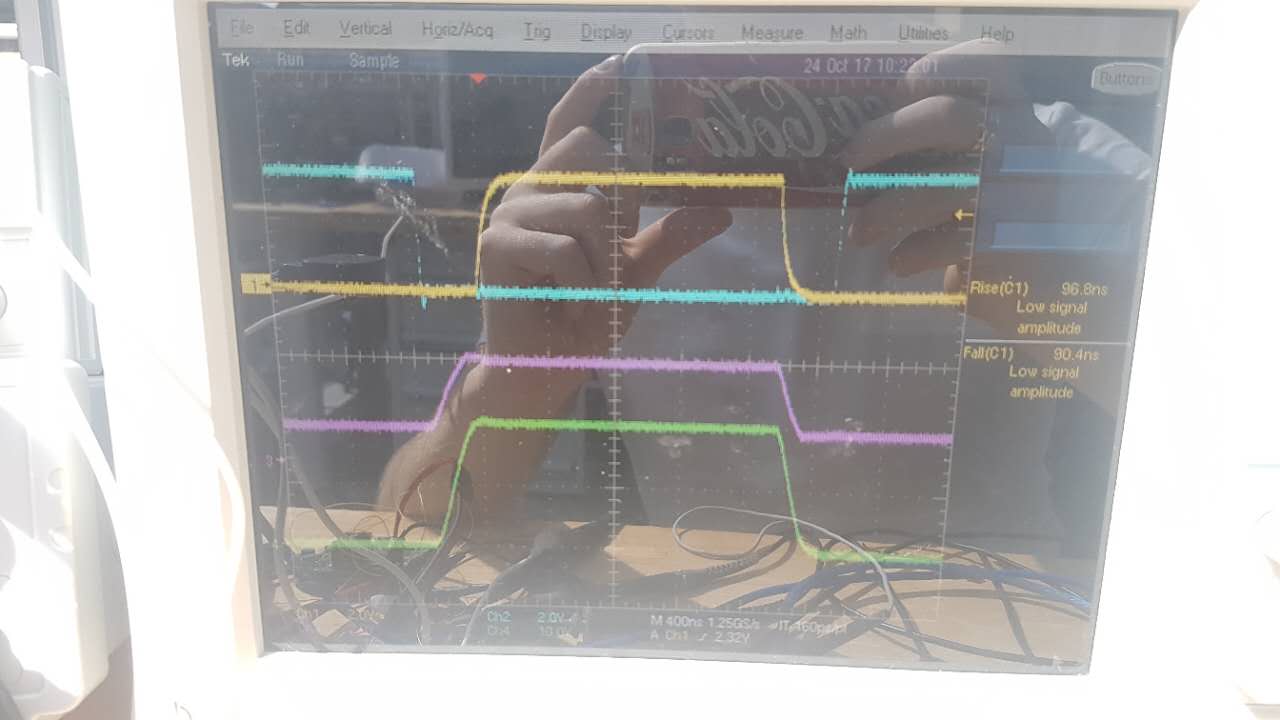
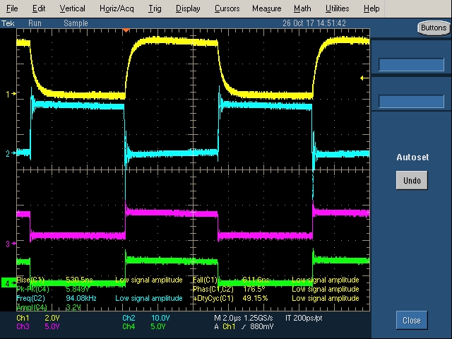
Input pwm is CMOS level, 500kHz , phase shift 180 degrees between Li and HI , 5 cycles of deadtime (at FSW).

The power pad is connected to 4 layers of ground plane. The boards stays around 34 degrees celcius. It is really the mosfet driver that heats up so much.

What can i do to solve this problem ? simply add some more cooling to it or slow down the switching ?

.

  • It is getting much hotter than what i get from my calculations:

    Any ideas?

  • Hi Thijs,

    Thanks for your question about UCC27211. Thanks for including everything as well. I will help you out with this issue.

    Are both FETs being damaged?

    Have you tried to probe Vgs during failure?
    Do you know the slew rate of your gate signal?

    Are you able to add a gate resistor from driver to FET?
    When no external gate resistor is employed between the driver and FET, the power is completely dissipated inside the driver package.
    With the use of external gate-drive resistors, the power dissipation is shared between the internal resistance of driver and external gate resistor.

    Also, I would like to take a look at your calculations in more detail.
    Can you send me the spreadsheet from your calculations screenshot?

    Thanks

  • calc.xlsxHello Jeff,

    I will do the measurements later today for you. I can mod a gate resistor in there. What value comes to mind ?

    I have a new batch of these drivers coming since the current one's I have come from a dubious source (ordered the 10 version instead of the 11, so I had to get the 11 version locally and the thermal pad looks a bit weird; Al-trough I doubt someone would go trough the trouble to fake these .... you never know in china).

    I think the fet's are still ok. They don't get hot on the thermal camera. I probed VGS before but will do again today and save a screenshot so I can post it here.

  • Fixed the problem.

    The low side mosfet blew up after a while. making the HS of the mosfet driver shorted to ground. Which blows up the mosfet driver.

    Fixed it by adding an external 100V 5A schottky diode in parallel with the low side mosfet (SS510).

    I had 60V 3A running trough this and did not have any issues.

    --

    I have another issue with this driver in a bi-directional high side low switch application which I will post in a new topic.

  • Is it recommended to also put another diode over the high side switch ?
  • Hi Thijis,

    Thanks for your calculation spreadsheet, just a couple comments:
    -θJCtop - is a parameter that is used to predict the thermal resistance when there is a perfect heaksink on top of the device. This thermal resistance uses a larger thermal potential to dissipate heat. Therefore all the heat is assumed to be dissipated from the top.
    -For the driver power consumption (with no switching) = Idd*VDD
    -For the driver power consumption during operation (with switching) = Iddo*VDD

    Thats good to hear you found a potential solution - this is a common solution to damped switch node ringing and to clamps to prevent the switch node from going negative. Its possible that an added resistance on LS gate might also delay the turn on/off of the LSFET enough to limit the possible ringing on the drain or undershoot the source and not make the FET fail as well. LS FET body diode loss comes from conduction losses as well as reverse recovery losses. Since you changed the forward voltage drop by using a low Rds_on schottky its possible the root cause is from forward diode conduction during DT and the reverse recovery spikes thereafter damage the LSFET which indefinitely charges the bootstrap and damages the driver.

    It will be helpful to know the root cause of the LSFET failure so that the potential fix can be looked at for both HS and LS FET. In general, a FETs body diode is required to prevent both FETs conducting at the same time - however this typically demonstrates performance inferior to that of an external Schottky diode. As a result, it is sometimes beneficial to use a Schottky diode as the anti-parallel diode bypassing the inherent body diode and resulting in an improvement of the conduction and recovery performance of the FET internal body diode.

    Do you have any more detail as to why the LSFET first failed?
    How much current do you have running through Q4 before it fails?
    any scope shots to explain things in more detail?


    Thanks,
  • It failed at low current of 30mA.

    With the diode fix we went up to 120 watt (40V 3A) with no issue. Below is the oscilloscope picture I had saved from before (no external diode).

    PWM input:
    Period: 4.25us (235kHz)
    duty cycle: 50%
    Dead band: 4 clock cycles
    yellow: PWM HI
    blue: PWM LI
    Purple: HB
    green: HS

    This is at 30mA load, VIN was 20V I think
    driver is 39 degrees celcius

    CH1,2,3 2v / div

    CH4 10v / div

    I can make a new capture of all the driver's output tomorrow.

    -- 

    On the oscilloscope (with the diode fix) you can still see ringing below ground. (measure at the input of the inductor) . My guess is that this went too much below ground and killed something in Q4.

    I'll show it on the oscilloscope tomorrow.

  • Hi Thijs,

    Sorry for my late reply, thanks for follow up info.

    To confirm, the scope shot above is with no diode fix?
    And you will send me a scope shot with the diode fix soon?

    Let me review your scope shot and get back to you asap, my response might be delayed a day due to a 2-day training I currently am in the middle of. However I will try to get a response to you before end of thursday.

    Thanks,
  • Pin: Probe mode:
    yellow: HS X10
    blue: LO X10
    Purple: HB X10
    green: HO X10

    Probe impedance: 1M

    Duty cyle 50%

    load current 6A

    Vsupply 30V

    I put a SS510 diode parallel over Q3 and over Q4

    Some notes: Last time I had the probe impedance on 50 ohm. This had a lot of effect on the Driver capacitor charging.

    At some times my VCC14 dipped and caused the mosfet driver to switch off (this was due to a setup error)

    Temperature at this load is 70 degrees celcius now. The shunt resistor is getting so hot; the driver and mosfets are at lower temperatures.

  • I notice that the driver will die in case VDD is gone while it is operational.
  • Hi Thijs,

    The probe impedance of 1MOhm gave cleaner results than the 50 Ohm?

    the LO-VSS waveform has lots of ringing on it. Can you zoom in on the falling transition?

    are the FETs damaged with the 6A load in the testing shot above?

    do you mean R5 when you say shunt resistor? what size is your shunt?

    Thanks,
  • Interesting development yesterday.

    Got in the "real" IC's from Arrow. Tested it and it works fine until you turn up the current to 200mA and it simply fails to turn on the mosfets properly.

    90% duty cycle (high side) and it does not let trough any current causing the output voltage to dip significantly. I probed HS, HB etc and the waveforms looks really weird (the pictures I posted before is the "Fake" IC).

    The real one does not follow the input signal properly and has weird ringing here and there. So we tried everything ... replacing mosfets, changing the HB capacitor with different values etc but nothing worked.

    Eventually out of ideas I just put the fake driver on there (since we had that working properly before) and voila! it works perfectly (waveforms I posted before).

    Also something we discovered with the "real" IC:

    - Half the frequency and it will take double the current before it fails to drive the high side mosfet properly (250 -> ~500mA) NOTE: The IC does NOT heat up so it is not an thermal issue. VCC14 has no dips.

    - Have switched the real IC out for a new one multiple times but the result was the same.

    - HO and LO waveforms always look weird, they do not "follow" the input signal like the "fake" one does. 

    The "fake" IC:

    - Works fine at 250 kHz 

    - Does not heat up much

    - Can handle 6A trough the mosfets with no issue (at 15 v)

    - Waveform performance is like posted above

    The fake IC is probably a lower specced TI mosfet driver IC in the same footprint or one from another brand and they changed the laser markings.

    The exposed pad on the fake IC looks weird (TI exposed pad is clean, sharp edges; the fake one has like a smaller pad and that was made bigger (by the looks of it) removing some of the epoxy enclosure to make the pad bigger. I'll post a picture later.

    But what now ? we have a "fake" IC that works well with consistent results; We have the real IC that does not work well consistently. 

    Now we need something to fix this. 

    In my mind a half bridge drive is really simple. Just follow whatever signal that is put in via LI HI and translate that to the correct voltages to drive the high side and low side mosfets.

    We are really surprised that the fake one works properly and the real one does not. At this point I ordered about 5 pin compatible drivers and I'm simply going to see which one works as expected and which one does not. I'm simply out of ideas now.

    - UCC27200QDDARQ1

    - HIP2101EIBZ

    - MIC4102YM

    - ISL2111ABZ

  • I have done all the requested measurements back to back in the exact same test setup. please see attached files.

    UCC27211DDAR fault analysis.pdf

    ALL_DATA.zip

    The real driver seems to fail to drive the high side mosfet properly. What is causing this ? How can I fix this ? do I need a different part or ???

  • Hi Thijs,

    Interesting indeed. Thanks for the through analysis and documentation! always good to see that.

    For the fake, I might be able to check the laser etching track down if/where this part came from TI. That might give a clue as to why you are seeing these results.

    The HSFET is unable to be switched with increasing converter current of only >250mA. From 171028_105905.jpg I can see HO skips every other cycle.

    For the real and weird results, can you probe (at 270mA load):
     
    HB-HS to see if the bootstrap is getting charged all the way
    HO-HS to see what the gate to source of the HSFET is doing
    as well as HO-VSS to know when the HSFET is supposed to switch.


    Thanks,

  • All the signals you mention are in the  screen-grabs from the oscilloscope. 
    What i need now is a solution. We have established already that it is not working.

    It would be good to track down the laser markings.

  • Hi Thijs,

    So far I am unable to find out where the potentially fake part came from however it may be in a assembly site that does not have a Lot Code. Can you send me a picture of the top of the potentially fake IC?

    Also, with further examination of your results I need more information. The only way the output is going to be as unstable as it looks is if the input supply goes outside spec. Vdd is rated at 17V and you have it at 14V. Its possible that its seeing a 3V spike in which HI is affected.

    With your PWM feedback disconnected (if there is one) and clean input signals at LI and HI to rule out it coming from the input side. As well as 50% duty cycle for easy buck output calculation.. Can you retake the scope shot with HI,HO, LI,LO with no BW limit. It will help to know what Vdd is doing on the falling edge of LO and rising edge of HO as well. Since this is where all the action is happening can you also take a zoomed in version of the scope shot?

    Thanks

  • Checked VDD14 and it is well within spec. No glitches to be found.

    As a last resort I put an external diode from VDD to HB and suddenly it works well up to 3A+. (this is with freshly soldered chip)

    HS signal is a clean square wave signal like you would expect of a high end driver like this. Much better than the fake one.

    But when I turned up the input voltage of the buck converter to 30V it started skipping pulses here and there (you can hear the coil make sound) and not too long after it died.

    VCC14 was well within spec at this moment.

    This must be a faulty batch right ? I can;t imagine this being a correct one.

    Note D3 and D4 were not on the board.

  • Hi Thijs,

    what died shortly after cranking up VIN to 30V, UCC27211?

    If the inductor is making an audible noise - is your inductor damaged?

    since your switching frequency is out of the 20kHz audible range its probably not due to this.

    since VIN is going up then inductor ripple is going down

    If Vdd is fine and If HS FET is skipping pulses after you turn up VIN then its likely something to do with the bootstrap or HI is skipping pulses. Since you added the external bootstrap diode in parallel with the internal bootstrap diode then its possible that the ripple current or bootstrap diode reverse recovery increased.

    Its also possible that HS node is being pulled below GND on LS deadtime and HB is being over-charged

    Can you scope HB-HS to see if the bootstrap is being over-charged?

    Thanks,

  • Due to the external diode mod the ringing at the HB point is quite high. Approaching 100V when VIN is ~33V. This causes HB-HS to get out of bounce ( = -24V). At this point it starts tripping (but that is understandable)

    Ignoring that;

    Why does it work when I add an external diode? is the internal one simply too weak ?

  • Hi Thijs,

    Since this part is a 120V gate driver its should at least be able to handle this voltage at the pins. However the max rating for HB-HS is 20V. HB has a negative voltage rating of -0.3V.

    why did the diode help is a good question.
    Some thoughts about adding another external BS:
    -larger reverse recovery
    -smaller losses with lower BS diode resistance and Vf
    -possibly faster BS charging or at least current divided BS charging

    Its also possible that with the addition of the external diode brings better charging and acting as a current divider taking some stress away form the internal diode which could occur from the out of boune HB-HS overcharging the bootstrap. If the bootstrap was getting overcharged by the out of bounce HB-HS then the interal bootstrap was getting damaged, this external bootstrap just reinforced the internal bootstrap.

    Thanks,
  • Doesn't this mean the IC does not work as shown in the datasheet ?
  • Hi Thijs,

    Is it possible that HB-HS out of bounds voltage ((24V in your case - where the abs max condition is HB-HS=20V) was the same voltage with the internal diode as was the case with the addition of the external diode. This would mean that the internal diode failed when HB-HS went outside of the DS abs max?

    Thanks,
  • At lower input voltages (20V) HS+ is 14v and HS- is around the same. This is only with the external diode added.

    The internal diode works up until 200mA load or so. Then it can not provide sufficient current it seems. So it fails.

    Is this my specific batch or is this a design fault in the chip?

  • Hi Thijs,

    BS diode current is independent of power train current.

    What do you mean by HS+ and HS-? .

    HS- (or lowest voltage) is -14V?

    if VIN is 20V then HS+ should be ~20V.

    As long as HO-HS is doing the right thing and not making HB-HS going out of bounds, HS can swing around all it wants.

    A scope of HB-HS with a differentail probe would clear things up along with HI, Vgs of HSfet.

    Are you able to look at this?

    Thanks,

  • Hi Thijs,

    Usually what can fail the boot diode, is the power train switching high dV/dt while the boot diode is still conducting current. For instance, if the HS turns on and there is still current charging the BS from LS being on then the BS will experience a greater loss due to reverse recovery which permanent damage might occur. Another example would be If there is very low LS on time and/or a boot cap that is much larger than required, that can also cause this issue.

    Thanks,

  • Hi Thijs,

    Is there any progress with your issue?

    Were you able to confirm this is diode failure? can you explain the failure in more detail?

    Thanks,