Hi LDO expert,
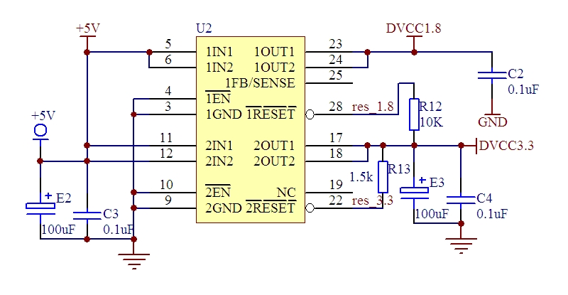
I meet a question about TPS767D318, you can see below schematic, which customer made a mistake - connected the res1.8V to DVCC_3.3.
customer understand this is not the correct design and they will modify in the next version design.
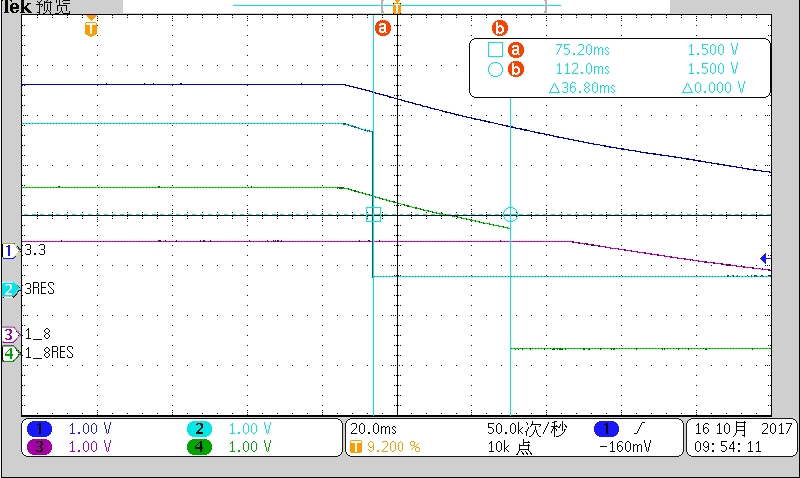
But based on this design, we found an interesting test result about the res_1.8 and you can find the test waveform as below.
test condition:
When vin 5V start to power down, then monitor the DVCC3.3 and res_3.3 and DVCC1.8 and res_1.8.
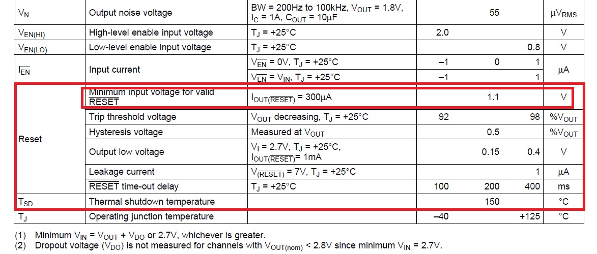
We can see from the test waveform the DVCC3.3 going down firstly and when the DVCC3.3 below 3.16V, then the res_3.3 going to logic "LOW".
Also, you can see the res_1.8 going down follow with DVCC3.3 (this is make sense becuase the res_1.8 been pulled up to DVCC3.3) before DVCC1.8 start to going down.
But, you can see the res_1.8 then going to logic "LOW" before the DVCC1.8 start to going down. could you please help comments on this test result? why?
Best Regards
IVEN XU